


Lund, Sweden – October 7, 2025 – AlixLabs, a pioneering Swedish semiconductor equipment startup, today announced that the United States Patent and Trademark Office (USPTO) has issued a Notice of Allowance for the continuation of its internally named “Tetris” patent. The new patent strengthens and broadens AlixLabs’ intellectual property portfolio, covering key innovations in selective side wall masking technology that integrate self-aligned double patterning (SADP) with the company’s proprietary Atomic Layer Etching-based Pitch Splitting (APS™) process.
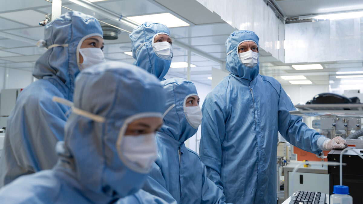
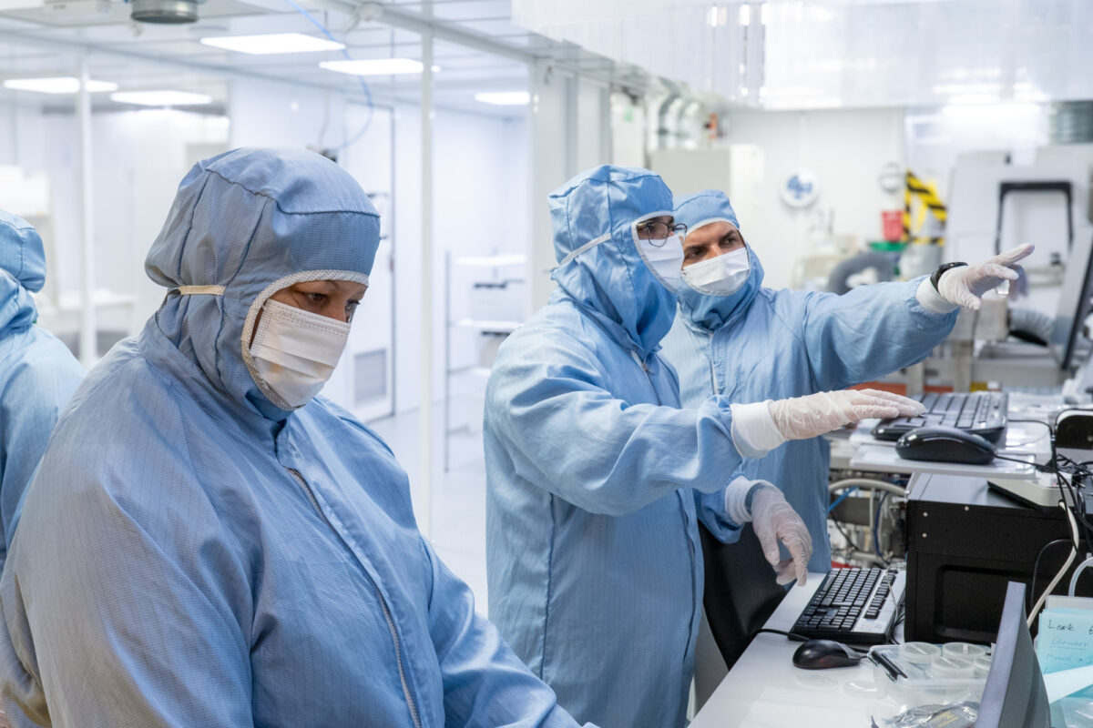
The continued development of next generation APS™ processes goes hand in hand with the company’s 300 mm platform with which it will engage in beta testing with leading IDMs & foundries. Activities such as these and a fortified IP portfolio further strengthens AlixLabs’ position as a leader in next-generation semiconductor manufacturing process technology for the Ångström Era.
Game-Changing Innovation for the Semiconductor Industry
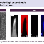
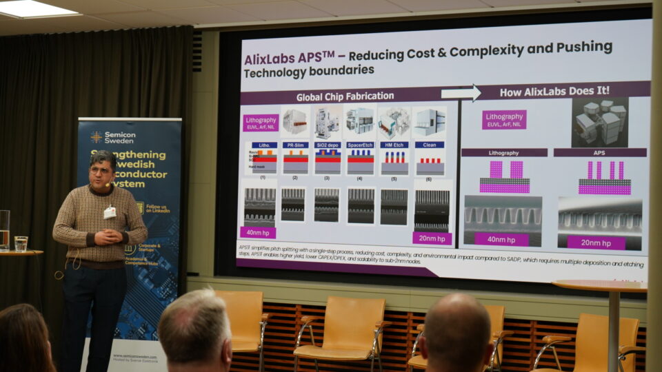
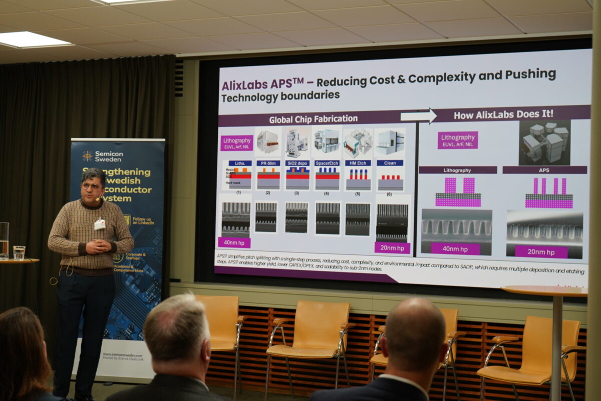
The invention arose from AlixLabs’ work on precise sidewall angle control in APS™, a critical aspect of advanced silicon processes. By combining classical SADP techniques with advanced APS™ methods, AlixLabs has developed a process that enhances topographical selectivity, cyclic process control, and overall performance.
The breakthrough enables semiconductor manufacturers to:
- Address patterning challenges at for DRAM and sub-7 nm logic nodes without using EUV lithography.
- Cut costs for fabless logic and memory chip manufacturing for AI, high bandwidth memory (HBM) and high-performance computing (HPC).
- Integrate APS™ technology into existing semiconductor production workflows while preserving compatibility with existing Process Design Kits (PDKs).
- Reduce capital and operational expenditure, while reducing greenhouse gas emissions at advanced technology nodes.
This new next generation APS™ process significantly lowers the barriers for adoption in high-volume manufacturing (HVM), offering manufacturers a flexible, cost-effective, and sustainable path forward.
Executive Statement
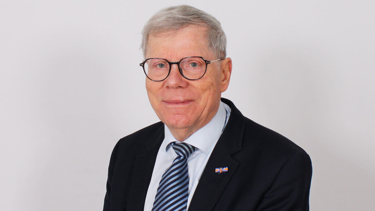
“This allowance is a major milestone for AlixLabs,” said Dmitry Suyatin, CIPO and Co-Founder of AlixLabs. “It validates our unique approach of merging classical and advanced techniques into a solution that is both practical and transformative for the semiconductor industry. With this patent, we not only strengthen our IP portfolio but also provide our customers with a pathway to more efficient and sustainable chip manufacturing at a lower cost.”
Next Steps
The patent is expected to be formally granted within the next one to three months following standard administrative steps. The patents that are part of the APS™ process will be used for customer demos in 2026 with AlixLabs’ APS™ beta cluster tool that is currently in design and manufacturing.

