


Funding will accelerate APS™ beta testing and scale-up toward advanced semiconductor manufacturing by 2027.
Lund, Sweden – November 18, 2025 – AlixLabs AB, a Swedish deep-tech company building a new generation of semiconductor manufacturing solutions, today announced the successful closing of a €14.1 million (SEK 155.2 million) Series A funding round. The investment will enable AlixLabs to accelerate development and scaling of its proprietary Atomic Layer Etching Pitch Splitting (APS™) technology – a disruptive process that enables more cost-effective leading-edge chip manufacturing.
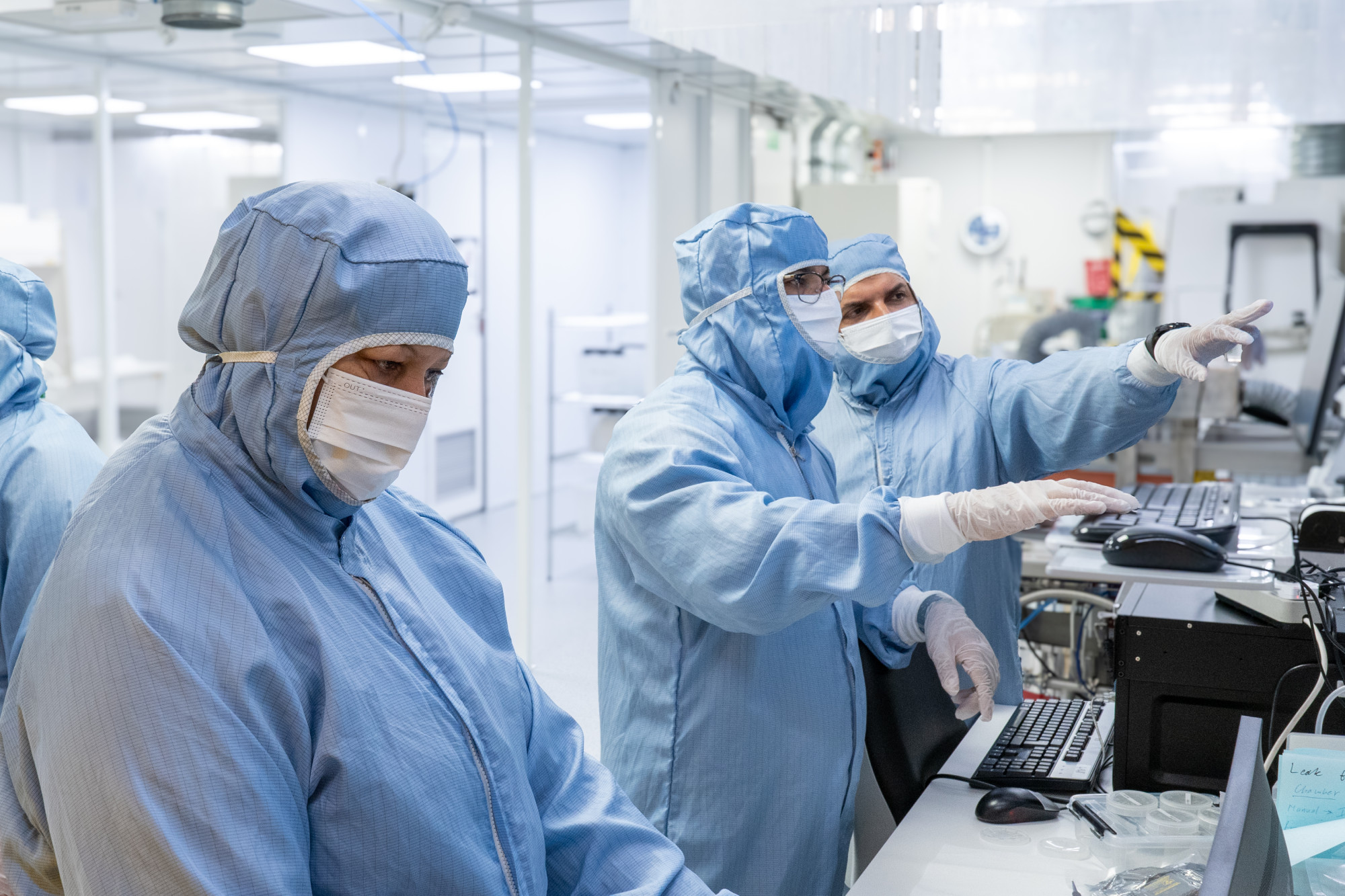
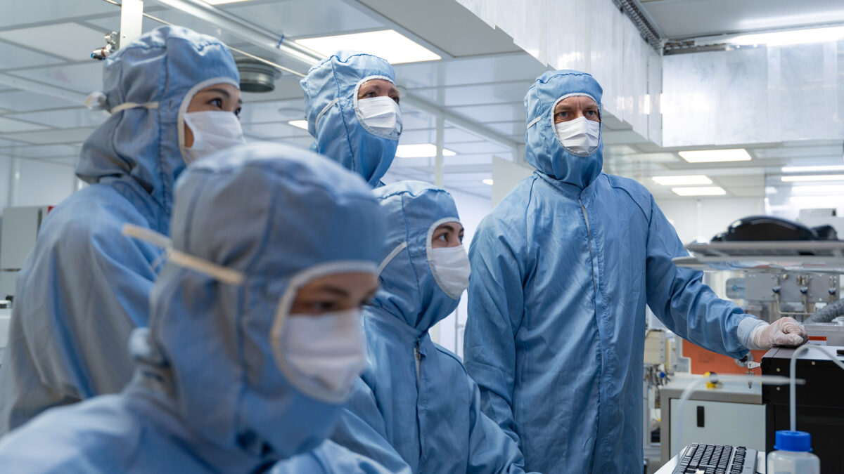
The funding round was led by Navigare Ventures, Industrifonden, and FORWARD.one, all of whom are reaffirming their commitment as long-term partners to AlixLabs’ growth journey. STOAF from Sweden as well as Global Brain, an independent Japanese venture capital firm that manages strategic funds and invests in semiconductor startups, joined the round. This further strengthens AlixLabs’ international reach and industry partnerships. The proceeds will be used to expand the company’s R&D and production capacity in Lund and the Netherlands, deepen collaboration with foundry partners, and initiate industrial deployment of APS™.
“This Series A enables us to transform our APS™ innovation from customer validation to industrial adoption,” said Jonas Sundqvist, CEO of AlixLabs. “We’re now entering an exciting phase where our focus turns toward beta testing with leading customers – a critical step on the path to full-scale manufacturing by 2027. Our technology has the potential to dramatically lower both energy use and costs per wafer, helping to make advanced semiconductor production more accessible.”
Investors Reaffirm Long-Term Commitment
“We’ve believed in AlixLabs’ vision from the start. Their technology tackles a critical bottleneck in semiconductor scaling and opens a path to more cost-efficient advanced chip manufacturing,” said Alex Basu, Chief Investment Officer at Navigare Ventures. “We’re excited to see APS™ validated with real customers – the next phase is all about bringing it onto the fab floor.”
“AlixLabs is a clear example of world-class innovation emerging from Sweden’s deep-tech ecosystem,” said Tobias Elmquist, Senior Investment Director at Industrifonden. “Their APS™ technology could fundamentally reshape the economics of advanced chipmaking while contributing to the industry’s sustainability goals.”
“We’re thrilled to continue supporting AlixLabs as they further progress to commercialization,” added Arjan Göbel, Partner at FORWARD.one. “With beta testing underway and manufacturing planned by 2027, AlixLabs is entering the most exciting chapter yet in its journey.”
A Sustainable Path for the Semiconductor Industry
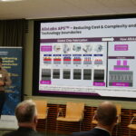
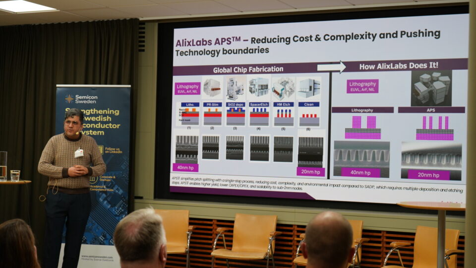
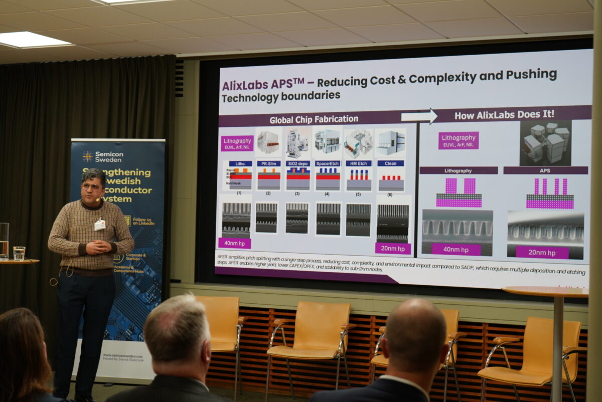
The global semiconductor industry faces rising capital intensity, soaring energy demands, and an urgent need to decarbonize production. AlixLabs’ APS™ platform offers a powerful new approach – enabling ultra-fine pitch splitting through atomic-scale precision etching, without the need for prohibitively expensive multi-patterning or exclusive reliance on EUV lithography. The result is lower process complexity, reduced power consumption, and smaller environmental footprint per wafer.
With its Series A funding secured, AlixLabs will accelerate APS™ beta testing with key customers starting 2026, targeting early manufacturing implementation by 2027.


