August 7, 2025
AlixLabs and NSS Water Partner to Revolutionize Sustainable Ultrapure Water Management in Semiconductor Manufacturing
Co-financed by ASCENT+ and leveraging Fraunhofer IPMS metrology for advanced defect control, the collaboration aims to cut costs, reduce environmental footprint, and enhance water recycling.
Stockholm, Sweden – August 7th, 2025 – AlixLabs and NSS Water are pleased to announce a strategic collaboration to develop sustainable and cost-effective ultrapure water (UPW) management solutions for chip production. Amid rising concerns over the semiconductor industry’s ever-increasing water consumption and regulatory pressure to reduce environmental impact, the two Swedish companies will team up to address this challenge.
The project value is approximately 28,000 euros, with funding coming from the European Union’s ASCENT+ program and is overseen by Fraunhofer IPMS (Institute for Photonic Microsystems.)
By integrating Fraunhofer IPMS’s state-of-the-art metrology expertise in advanced defect and contamination control, the partnership aims to improve and elevate water recycling methods, reduce chemical usage, and optimize overall process efficiency – paving the way for smarter water solutions in a water-constrained future.
According to industry data, the semiconductor sector has experienced a 20–30% increase in water consumption in recent years, with the average chip manufacturing facility using up to 10 million gallons of UPW daily – an amount equivalent to the daily water needs of a city of 300,000 people. Producing UPW traditionally comes at a significant cost: it can be 60 to 350 times more expensive than drinking water due to the intensive energy and chemical processes required. This is the challenge NSS Water addresses with its nano-pure water (NPW).
The semiconductor industry’s water consumption is projected to keep increasing due to more advanced plants with higher consumption coming online in the coming years. Additionally, 40% of chip production facilities are projected to be located in high-water-risk areas by 2030, meaning the need for data-driven, circular water strategies has never been more critical.
“Water is the lifeblood of our planet and the backbone of the semiconductor industry,” says Reza Jafari Jam, Research Director at AlixLabs. “This collaborative research on water conservation not only safeguards a finite resource but fuels innovation, ensuring sustainable growth and technological advancement. We push the semiconductor industry to be more sustainable with our APS™ patterning process technology and our collaboration with NSS Water will further solidify our position as an enabler tomorrow’s green semiconductor production.”
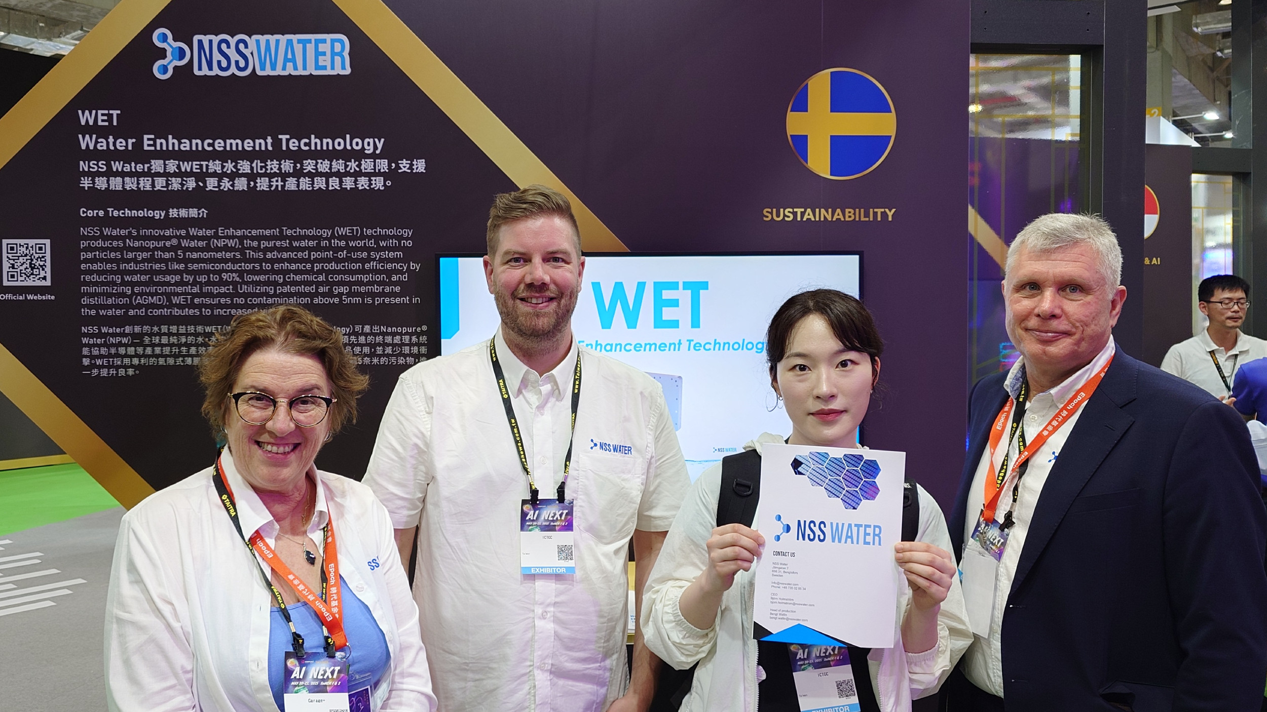
“We are happy to expand our collaboration with AlixLabs and Fraunhofer,” says Björn Holmström, CEO at NSS Water. “The importance of advanced metrology will help us provide a platform that improves the water infrastructure used by AlixLabs and other advanced semiconductor players. With this project, we get to benchmark our NPW on 300-millimeter wafers as well as have the wafers cleaned with NPW by Fraunhofer.”
Through this partnership, AlixLabs and NSS Water are combining their respective strengths in innovative water treatment, advanced analytics, and semiconductor manufacturing know-how to develop solutions that significantly reduce water usage, lower operational costs, and bolster sustainability. Fraunhofer IPMS’s involvement ensures precise contamination and defect control, further enhancing the effectiveness of the recycling and purification processes.
Co-financed by the European Nanoelectronics Access program ASCENT+, which provides a direct gateway to Europe’s global-scale Nanoelectronics Research Infrastructure, granting researchers, SMEs, and PhD candidates access to state-of-the-art capabilities. The project is an important step in positioning AlixLabs, NSS Water and the European Union at the forefront of sustainable semiconductor manufacturing innovations.
About AlixLabs
Established in 2019 in Lund, Sweden, AlixLabs emerged as a spin-off from Lund University with a mission to enable the cost-effective and energy-conscious fabrication of semiconductors, particularly logic and memory components. AlixLabs boasts patented recognition for its groundbreaking APS™ technique, a process that achieves nanostructure division through etching. This method holds approved patents across the USA, Taiwan, and Europe. The APS™ acronym signifies ALE Pitch Splitting, leveraging ALE (Atomic Layer Etching), a plasma-based dry etching cyclic methodology. For more details, please visit www.alixlabs.com