


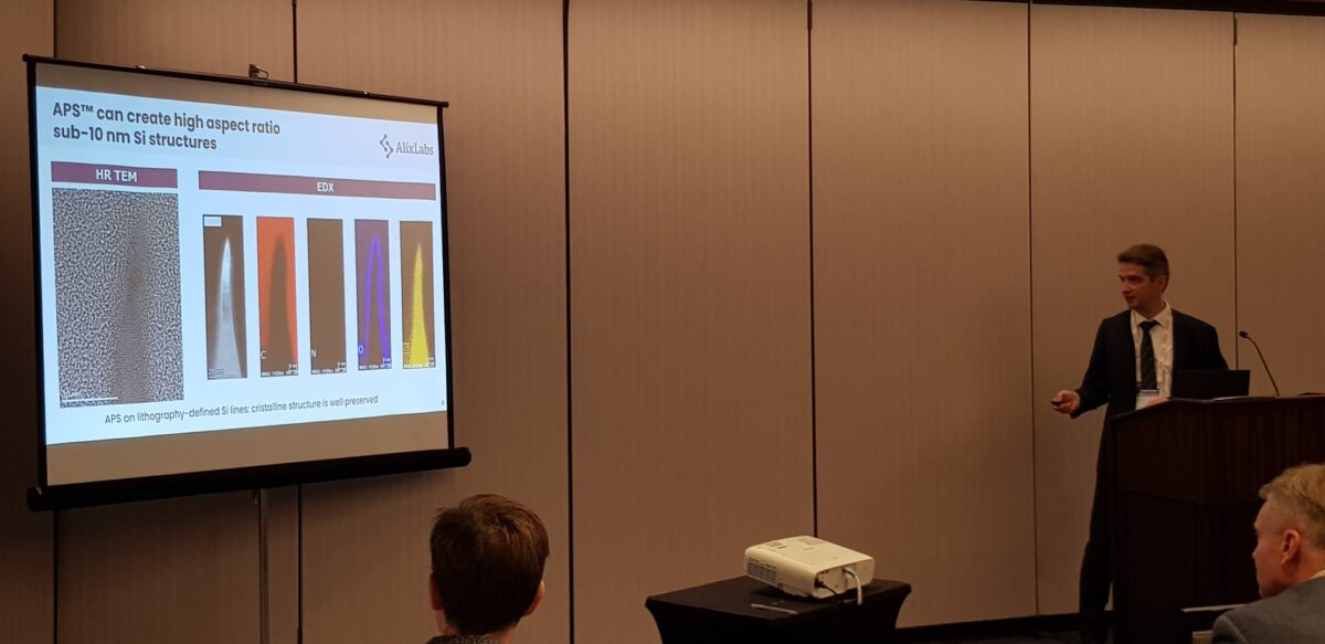
AlixLabs is pleased to announce that Dr. Dmitry Suyatin, CIPO and Co-Founder, has presented the company’s latest advances in APS™ (Atomic Layer Etching Pitch Splitting) at the 248th Electrochemical Society (ECS) Meeting held in Chicago, October 12–16, 2025.
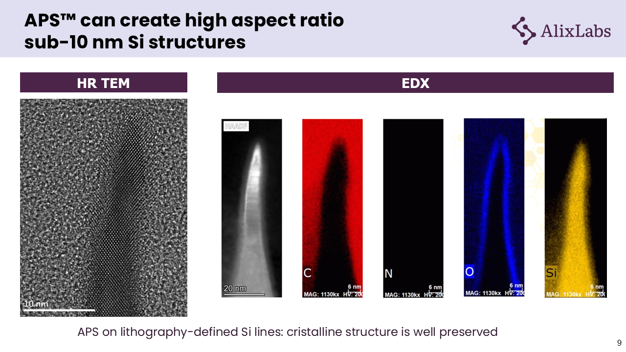
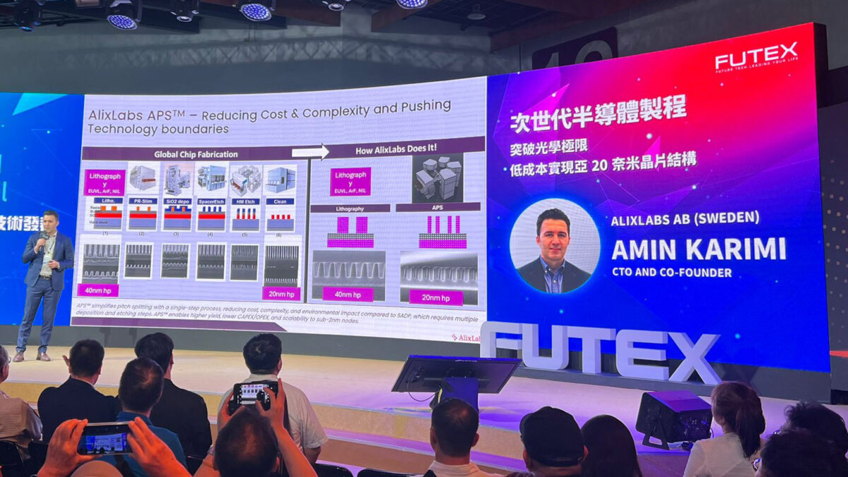
During the session, Dr. Suyatin highlighted new experimental results demonstrating high-aspect-ratio (HAR), narrow-fin patterning on bulk silicon achieved using conventional immersion lithography at a 193-nanometer wavelength. These results further confirm the viability of APS™ as an innovative method for extending fine-pitch patterning capabilities using existing lithography infrastructure.
By enabling advanced logic patterning without the need for next-generation scanners, APS™ offers a significant opportunity to reduce process complexity and cost, paving the way for broader access to advanced semiconductor manufacturing technologies.
“These new APS™ results – demonstrating high-aspect-ratio narrow-fin (CD < 10 nm) patterning on bulk silicon – go hand in hand with our recent patent successes,” said Dmitry Suyatin, CIPO and Co-Founder of AlixLabs. “Together, they validate APS™ as both a technically sound and strategically protected innovation in semiconductor manufacturing. As we prepare to install our beta tool that will become operational in fall 2026, we’re excited to take APS™ from lab-scale to production-grade refinement. Each step brings us closer to making advanced logic manufacturing simpler, more accessible, and more cost-efficient for the global industry.”
The advances presented at ECS reflect AlixLabs’ long-term mission to lower the threshold to advanced logic production, supporting a more sustainable, affordable, and globally accessible semiconductor ecosystem.
This research has been led by Dr. Dmitry Suyatin and Dr. Intu Sharma, whose work continues to push the boundaries of patterning innovation.

