AlixLabs is proud to announce its participation at SPIE Advanced Lithography + Patterning, the semiconductor industry’s leading forum for breakthroughs in optical and EUV lithography, patterning technologies, and process integration.
We are excited to share that two of our submitted abstracts has been accepted for oral presentation at the SPIE Advanced Lithography + Patterning conference, one in partnership with UMC:
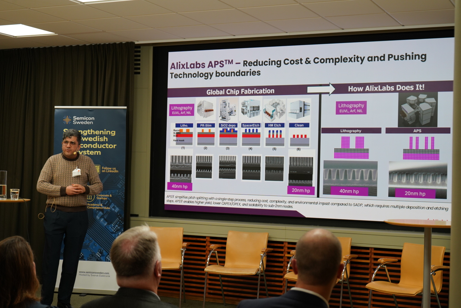
- Atomic layer etching pitch splitting (APS™) for nanoimprint lithography: Combining simplicity, precision, and sustainability
Date/Time: 24 February 2026, 11:10–11:30 AM (PST)
Presenter: Reza Jafari Jam, Research Director at AlixLabs
This talk presents new results on applying AlixLabs’ APS™ atomic-layer–etch-based pitch splitting to Si structures1. We demonstrate sub-13 nm half-pitch patterning and discuss how APS™ can offer a more cost-effective and sustainable alternative to conventional multi-patterning routes.
Link to abstract: SPIE - Self-aligned quadruple patterning made simple: Extending the applications of atomic layer etch-induced pitch splitting (APS™)
Date/Time: 24 February 2026, 11:50 AM–12:10 PM (PST)
Presenter: Robin Athle, Principal Researcher at AlixLabs
In this presentation, we extend APS™ toward a streamlined alternative to self-aligned quadruple patterning (SAQP) in collaboration with United Microelectronics Corporation (UMC). The process enables a 4× density increase using a simplified three-step flow, delivering ~12 nm half-pitch structures while reducing complexity versus traditional SAQP schemes.
Link to abstract: SPIE
SPIE Advanced Lithography + Patterning will be held in San Jose, California, bringing together global experts in lithography and nanopatterning.
We look forward to connecting with partners, customers, and fellow researchers at the symposium.
If you plan to attend, we warmly invite you to join our sessions on February 24 and reach out to schedule a meeting with the AlixLabs team.
Footnote:
- The Si structures are patterned by Canon Inc.’s nanoimprint lithography (NIL) ↩︎


