
June 23, 2026
AlixLabs launches Sax Forma for the Ångström era
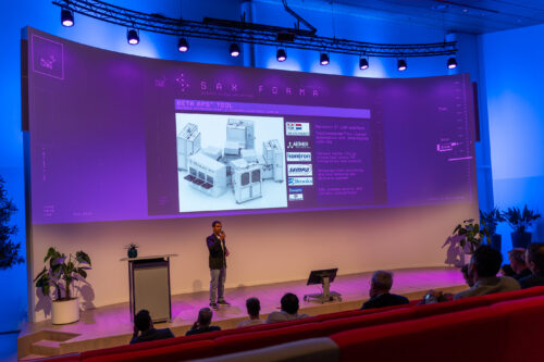
Lund, Sweden – June 23, 2026 – AlixLabs AB, a semiconductor equipment company specializing in advanced etch and patterning technologies, launched Sax Forma, an APS™ System, the company’s first commercially available equipment platform for Atomic Pitch Splitting (APS).
The launch marks AlixLabs’ transition from technology validation toward customer engagement, process integration, and industrial equipment deployment. Sax Forma is designed to bring APS™ into advanced semiconductor manufacturing flows, where continued scaling increasingly depends on reducing patterning complexity.
“With Sax Forma, we are taking APS from validated technology to a commercially available equipment platform,” said Jonas Sundqvist, CEO at AlixLabs. “This is an important step for AlixLabs as we begin deeper customer engagement around how APS can be integrated into existing manufacturing flows and support the industry’s continued scaling roadmap.”
Patterning has become one of the most cost-sensitive and technically demanding areas of advanced chip production, as scaling increasingly requires multi-patterning, additional process loops, and tighter control of critical dimensions, overlay, film thickness, and profile. APS addresses this challenge as a complementary patterning system inserted downstream of established lithography-based process flows, including DUV, EUV, and nanoimprint lithography.
By increasing pattern density without requiring a new lithography platform, APS enables fabs to reduce patterning complexity while preserving existing fab infrastructure and manufacturing investments.
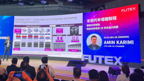
Sax Forma builds on APS demonstrations using industry-relevant silicon, including 300 mm silicon wafers from UMC and Intel FinFET test silicon. On the Intel test silicon, APS reduced the half-pitch from 25 nanometers to 12.5 nanometers, demonstrating performance relevant to geometries associated with the 3-nanometer class. In laboratory settings, AlixLabs has also shown that sequential APS processing can enable further half-pitch reduction, pointing toward future scaling as the industry moves toward 2-nanometer, Ångström-class nodes, and beyond.
Together, these demonstrations support AlixLabs’ core claim: that APS can enable controlled half-pitch refinement in dense, line-based patterning layers without relying on repeated spacer-based process loops.
“APS is designed to complement lithography by adding a controlled pitch-splitting step after the initial pattern has been defined,” said Amin Karimi, CTO at AlixLabs. “The objective is to reduce patterning complexity while preserving compatibility with established process flows. That integration model is central to how we see APS being adopted by semiconductor manufacturers.”
Sax Forma is being industrialized together with VDL ETG Projects, AlixLabs’ partner for system integration and high-tech equipment manufacturing. Building on the collaboration announced earlier this year, VDL ETG Projects is supporting the transition of APS from advanced R&D and process validation into industrial equipment, drawing on its experience in design, engineering, realization, and scale-up from first-of-a-kind systems toward batch manufacturing.
AlixLabs has also built a strong and growing patent portfolio around APS and its equipment platform. The core APS principle is patent protected in key semiconductor markets including the EU, the United States, and Taiwan, while the company expects its process optimization work and hardware innovations to be covered by nine and eleven patent families, respectively, by the end of the year.
Sax Forma enters the market as AlixLabs’ Beta system, intended for customer evaluation, integration work, and validation in production-like environments. As the first commercially available APS equipment platform, it forms the basis for the company’s planned Gamma platform, targeted for 2028.
With Sax Forma, AlixLabs is bringing APS to market as a semiconductor equipment platform that offers a solution to one of the industry’s central scaling challenges: reducing patterning complexity on the path toward the Ångström era.
About AlixLabs
Established in 2019 in Lund, Sweden, AlixLabs emerged as a spin-off from Lund University with a mission to enable the cost-effective and energy-conscious fabrication of semiconductors, particularly logic and memory components. AlixLabs boasts patented recognition for its groundbreaking APS™ technique, a process that achieves nanostructure division through etching. This method holds approved patents across the USA, Taiwan, and Europe. The APS™ acronym signifies ALE Pitch Splitting, leveraging ALE (Atomic Layer Etching), a plasma-based dry etching cyclic methodology.
May 7, 2026
AlixLabs to host APS™ System Launch Event in Eindhoven on June 4
Lund, Sweden – May 7th, 2026 – AlixLabs will host the official launch event for its APS™ (Atomic Pitch Splitting) System, gathering guests from across the semiconductor ecosystem at High Tech Campus Eindhoven in the Netherlands.
The event marks an important milestone in AlixLabs’ transition from technology validation toward industrial deployment, as the company moves to introduce APS™ as a new patterning approach for advanced semiconductor manufacturing.
As advanced semiconductor manufacturing faces increasing challenges related to patterning complexity, process cost and manufacturability, APS™ has been developed to enable advanced pitch division through Atomic Layer Etching-based integration schemes aimed at simplifying multi-patterning flows and reducing process complexity in advanced semiconductor manufacturing.
During the event, AlixLabs will present the APS™ system architecture, recent development progress and the broader industrial implications of the technology, including process integration, manufacturability and future scaling opportunities.
“APS™ has been developed with manufacturability and industrial scalability in mind from the beginning,” said Jonas Sundqvist, CEO and Founder of AlixLabs. “This event represents an important step as we continue expanding our ecosystem engagement and move toward future industrial implementation.”
The APS™ System Launch Event will take place on June 4, 2026 at High Tech Campus Eindhoven in the Netherlands, with registration opening at 15:00 CEST and the main program running from 16:00 to 18:00, followed by networking.
Event details:
Date: June 4, 2026
- Location: High Tech Campus Eindhoven, The Netherlands
- Registration opens: 15:00 CEST
- Main program: 16:00–18:00 CEST
- Networking session: 18:00 onwards
Due to limited venue capacity, registration is required. Additional information and registration details are available here:
About AlixLabs
Established in 2019 in Lund, Sweden, AlixLabs emerged as a spin-off from Lund University with a mission to enable the cost-effective and energy-conscious fabrication of semiconductors, particularly logic and memory components. AlixLabs boasts patented recognition for its groundbreaking APS™ technique, a process that achieves nanostructure division through etching. This method holds approved patents across the USA, Taiwan, and Europe. The APS™ acronym signifies ALE Pitch Splitting, leveraging ALE (Atomic Layer Etching), a plasma-based dry etching cyclic methodology.
April 14, 2026
AlixLabs Closes 15 M EUR Series A with Strategic Investment from Stephen Industries
Lund, Sweden – April 14th, 2026 – AlixLabs, a pioneer in Atomic Layer Etching (ALE) technology for next-generation semiconductor manufacturing, today announced that it closed its 15 million euro Series A in the first quarter of 2026 following a strategic investment from Stephen Industries, a Finnish investment company with a strong track record in scaling advanced technology ventures.
In November 2025, AlixLabs announced that Global Brain and key institutional investors had subscribed to its Series A to the tune of 14,1 million euro, with the difference to the 15 million total remaining open until the first quarter of 2026.
The investment marks a strategic milestone for AlixLabs as it continues to develop its proprietary ALE solutions with especially its flagship APS™ (Atomic Pitch Splitting) technology aimed at enabling more precise, efficient, and cost-effective semiconductor fabrication.
A key dimension of the partnership is the involvement of Kustaa Poutiainen of Stephen Industries, whose experience in building and scaling deep-tech companies brings significant strategic value. Poutiainen previously played a central role in the growth of Picosun, a Nordic Atomic Layer Deposition (ALD) company that became a global leader in its field. Given the close technological relationship between ALD and ALE, this track record is particularly relevant to AlixLabs’ mission.
“Stephen Industries brings deep industrial expertise and a proven ability to scale companies in adjacent technology domains,” said Jonas Sundqvist, CEO of AlixLabs. “Kustaa’s experience with Picosun is especially valuable as we move from development toward broader commercialization of our APS™ platform.”
Atomic Layer Etching is widely seen as a critical enabler for future semiconductor nodes, complementing ALD processes by allowing atomic-scale precision in material removal. As device architectures become increasingly complex, ALE is expected to play a central role in manufacturing.
“AlixLabs operates in a highly promising space within semiconductor process technology,” said Kustaa Poutiainen, Chairman and President of Stephen Industries. “Having seen firsthand how ALD evolved from a niche innovation to a critical industry standard, I see strong parallels with ALE. AlixLabs has the potential to follow a similar trajectory.”
The new funding will be used to accelerate product development, expand technical capabilities, and strengthen partnerships with semiconductor manufacturers.
This investment reinforces AlixLabs’ position as a key innovator in the European semiconductor ecosystem and supports its ambition to become a global leader in Atomic Layer Etching.
April 7, 2026
AlixLabs and VDL ETG Projects Announce MoU for APS™ Patterning Technology Industrialization

Lund, Sweden – April 7th, 2026 – AlixLabs AB, a semiconductor equipment company specializing in Atomic Layer Etching (ALE) innovations, today announced that the company has signed a Memorandum of Understanding (MoU) with VDL ETG Projects, part of VDL Groep, to advance the production of APS™ (Atomic Pitch Splitting) equipment.
The agreement marks a significant step toward industrializing AlixLabs’ APS™ technology, enabling scalable manufacturing solutions for advanced semiconductor patterning.
APS™ is designed to address critical challenges in next-generation semiconductor fabrication by enabling precise pitch splitting through atomic layer etching. This approach offers a cost-efficient and energy-conscious alternative to increasingly complex multi-patterning and EUV-based lithography.
Under the MoU, VDL ETG Projects will play a key role in developing and manufacturing the industrial APS™ tools, leveraging its expertise in system integration and high-tech equipment manufacturing. The collaboration aims to transition APS™ from advanced R&D into robust, production-ready systems for semiconductor fabs.
“This MoU represents an important milestone for AlixLabs as we move from technology validation toward industrial deployment,” said Jonas Sundqvist, CEO of AlixLabs. “Partnering with VDL ETG Projects strengthens our ability to scale APS™ and bring a new patterning paradigm to the semiconductor industry. Their industrialization capabilities are a strong complement to our process innovation.”
Sorin Stan, Senior Director for Emerging Technologies at VDL ETG Projects added:
“The implementation of AlixLabs’ research in the manufacturing processes for advanced semiconductor devices will contribute to overall cost reductions and increased production speeds. The industrialization of the first-of-a-kind APS™ equipment currently under development for AlixLabs will play an essential role in fulfilling the next-node strategies at many of their customers.”
The partnership reflects a shared ambition to accelerate the adoption of innovative patterning technologies and support the semiconductor industry’s need for sustainable scaling.
About AlixLabs
Established in 2019 in Lund, Sweden, AlixLabs emerged as a spin-off from Lund University with a mission to enable the cost-effective and energy-conscious fabrication of semiconductors, particularly logic and memory components. AlixLabs boasts patented recognition for its groundbreaking APS™ technique, a process that achieves nanostructure division through etching. This method holds approved patents across the USA, Taiwan, and Europe. The APS™ acronym signifies ALE Pitch Splitting, leveraging ALE (Atomic Layer Etching), a plasma-based dry etching cyclic methodology.
About VDL ETG Projects
As part of VDL Groep of The Netherlands, VDL ETG Projects has a proven track record in supporting innovative companies in the transition from the feasibility to the design, engineering, and realization of their equipment. With all needed expertise under one roof, VDL ETG Projects scales up the equipment manufacturing from first-of-a-kind units to batch manufacturing, and further to turnkey realization of complex production lines. VDL Groep is an industrial conglomerate headquartered in Eindhoven, The Netherlands. It was founded in 1953 and consists currently of more than 100 specialized companies employing together more than 14,000 employees in 20 countries and operating in several industrial sectors. For more details, please visit https://www.vdlgroep.com/en.
February 26, 2026
AlixLabs Granted EU Trademark Registration for Power ALE
Lund, Sweden – 26 February, 2026 – AlixLabs AB today announced that the European Union Intellectual Property Office (EUIPO) has formally granted registration of the Power ALE trademark (EU Trademark No. 019250271), reinforcing the company’s expanding intellectual property portfolio in advanced semiconductor manufacturing technologies.
The registration was recorded on 5 February 2026 by the EUIPO and secures protection for the Power ALE brand across the European Union.
Power ALE is trademarked across a broad range of semiconductor-related goods and services, reflecting AlixLabs’ vertically integrated approach to innovation and commercialization. The registration covers, among other areas:
- Chemical substances and materials for use in semiconductor manufacturing, including etchants, oxidants, thin-film deposition materials and semiconductor silicon
- Semiconductor manufacturing machinery and wafer processing equipment, including etching systems and substrate processing machines
- Semiconductors, integrated circuits, wafers, optoelectronic devices and related software
- Processing and custom manufacturing services for semiconductor components, wafers, nano-scale materials and nanostructures
- Research, technical consultancy, and design services in semiconductor process technology, integrated circuits and nano-scale materials
The breadth of the registration underscores Power ALE’s role within AlixLabs’ technology ecosystem and aligns with the company’s Atomic Layer Etching-based process innovations, including its previously announced APS™ (Atomic Layer Etching Pitch Splitting) trademark.
“Securing EU-wide trademark protection for Power ALE marks another important milestone in strengthening AlixLabs’ intellectual property platform,” said Dmitry Suyatin, Chief Scientific Officer (CSO) of AlixLabs. “Power ALE represents a strategic extension of our Atomic Layer Etching expertise, covering not only process technology but also materials, equipment, software and semiconductor devices. By protecting the brand across this full value chain, we are reinforcing our long-term commitment to industrialization and commercialization of advanced nanoscale manufacturing technologies in Europe.”
The registration provides legal protection for the Power ALE brand through 22 September 2035 and supports AlixLabs’ continued engagement with semiconductor manufacturers, equipment partners, and research institutions across the EU and internationally.
With both APS™ and Power ALE™ now formally protected trademarks within the European Union, AlixLabs continues to build a structured brand architecture around its proprietary Atomic Layer Etching innovations – positioning the company for expanded partnerships, licensing opportunities and future product introductions.