April 10, 2025AlixLabs to Demonstrate APS™ on 300-millimeter UMC wafers at the 2025 CMC ConferenceAtomic Layer Etching Pitch Splitting (APS) proven on more industry-leading wafers, doubling fin density and proving flexibility without EUV.
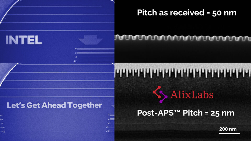
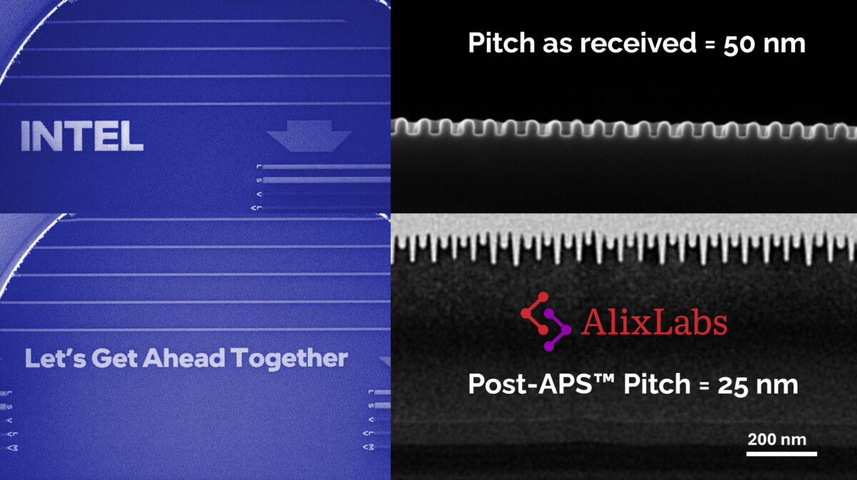
February 7, 2025AlixLabs to Showcase Latest APS™ Findings at SPIE Advanced Lithography + PatterningSwedish semiconductor startup to demonstrate 3-nanometer class FinFET structures made with APS™ on Intel Silicon at trade show.

