May 7, 2026AlixLabs to host APS™ System Launch Event in Eindhoven on June 4Join us as we officially launch APS™ in one of Europe's semiconductor hotbeds.
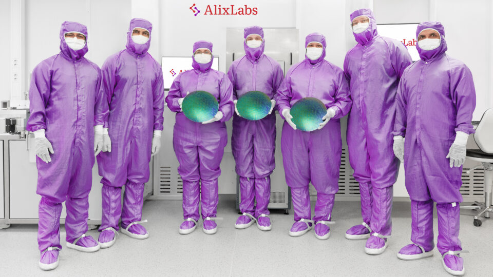
April 14, 2026AlixLabs Closes 15 M EUR Series A with Strategic Investment from Stephen IndustriesFinnish investor completes AlixLabs Series A, bringing ALD expertise.
April 7, 2026AlixLabs and VDL ETG Projects Announce MoU for APS™ Patterning Technology IndustrializationAlixLabs announces that it has signed a Memorandum of Understanding with VDL ETG Projects to scale APS™ equipment.
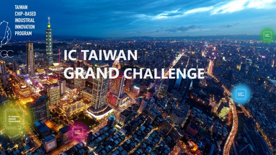
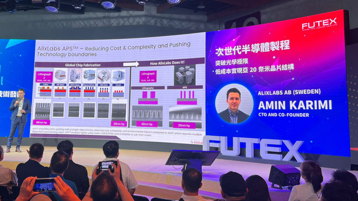
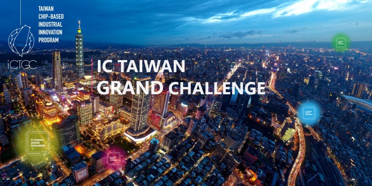
August 28, 2025AlixLabs Chosen as a Winner in IC Taiwan Grand ChallengeAlixLabs has been selected as a winning company from the third batch of the IC Taiwan Grand Challenge, an international competition that recognizes groundbreaking innovations in semiconductor and related technologies.


