

October 1, 2026
AlixLabs begins APS™ technology evaluation within the NanoIC pilot line
Lund, Sweden – October 1, 2026 – AlixLabs AB, a Swedish semiconductor equipment company developing Atomic Layer Etch Pitch Splitting (APS™), starts a six-month evaluation project to assess the potential of its APS™ technology for advanced semiconductor patterning within the NanoIC pilot line, coordinated by imec. The project will evaluate the technology in an advanced pilot manufacturing environment.
The evaluation will examine the performance of AlixLabs’ APS™ technology. The project will combine AlixLabs’ atomic layer etch-based pitch splitting process with imec’s advanced lithography, process integration and metrology capabilities, made available through the infrastructure of the NanoIC pilot line.
APS™ is a pitch-splitting process in which pre-patterned structures are selectively divided to create two lines from one original feature, doubling pattern density. The process uses atomic layer etching to provide highly controlled material removal and is intended to reduce the number of process steps compared with conventional multiple-patterning approaches such as litho-etch-litho-etch, self-aligned double patterning and self-aligned quadruple patterning.
For the evaluation, imec will prepare line-and-space structures with feature sizes comparable to some of the most advanced semiconductor processes in production today. The structures will be characterized before being sent to AlixLabs for APS™ process development. AlixLabs will initially develop and assess the process on coupons before transferring selected process conditions to full wafers.
The resulting structures will be evaluated against key semiconductor patterning metrics including critical dimension and critical dimension uniformity, line-edge and line-width roughness, pitch walking, profile and recess, and stochastic defectivity. Following APS™ processing, full wafers will be returned to imec for characterization using imec’s metrology and methodology baselines.
“This evaluation gives AlixLabs the opportunity to assess APSTM in a highly relevant and rigorous semiconductor pilot line environment,” said Jonas Sundqvist, CEO of AlixLabs. “The strategic value for us is the ability to generate data using imec’s established expertise, metrology and process methodology. It is an important step in demonstrating where APSTM can contribute within advanced patterning and in advancing our role in the European semiconductor technology ecosystem.”
The project marks a further step in AlixLabs’ transition from development of APS™ as a novel patterning concept toward evaluation within advanced semiconductor process flows. AlixLabs aims to generate performance data across both process-development structures and full wafers.
“The NanoIC Pilot Line is designed to help innovative semiconductor technologies mature in an advanced pilot manufacturing environment. Our collaboration with AlixLabs combines its APS™ technology with imec’s expertise in lithography, process integration, and metrology to assess the potential of a novel patterning approach using industry-relevant metrics. This project highlights the value of ecosystem collaboration in accelerating innovation, reducing development risk, and strengthening Europe’s semiconductor technology leadership,” said Giuseppe Fiorentino, Program Manager at imec.
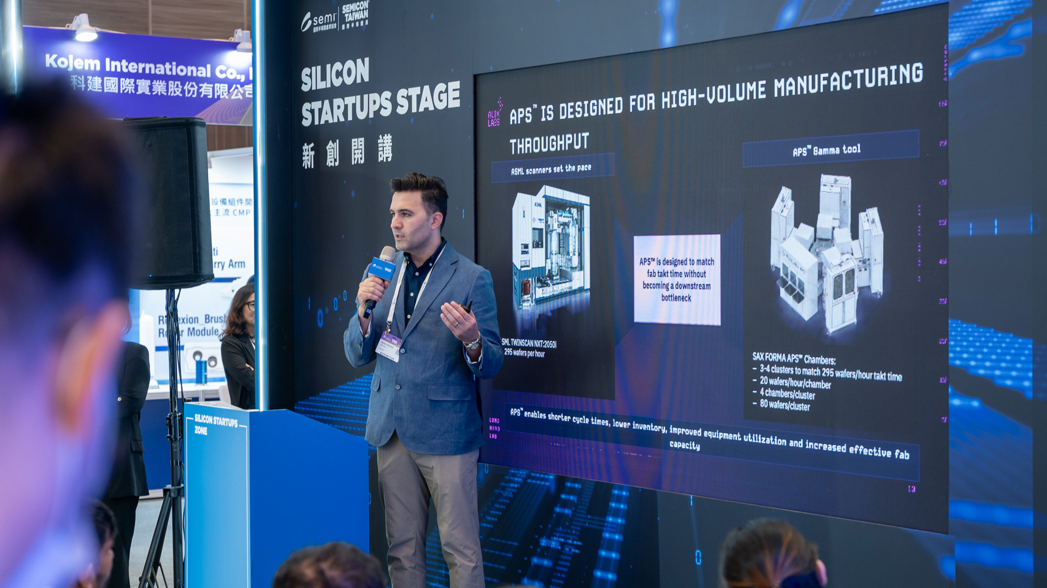
Looking ahead, this evaluation represents an important step toward AlixLabs’ longer-term objective of deploying its Sax Forma APS™ platform into high-volume manufacturing (HVM) environments. This next level of validation at imec has also been specifically requested by several potential customers as part of their assessment of APS™ and its readiness for integration into advanced semiconductor manufacturing.
AlixLabs intends to use the resulting process data, integration understanding and full-wafer performance evidence to advance APS™ from technology evaluation toward industrial qualification. Successful results would provide an important foundation for the next phase of development, including further process integration, equipment qualification and direct engagement with semiconductor manufacturers as AlixLabs works toward bringing APS™ into HVM.
About the project
This work was enabled by the NanoIC pilot line. The acquisition and operation are jointly funded by the Chips Joint Undertaking, through the European Union’s Digital Europe (101183266) and Horizon Europe programs (101183277), as well as by the participating states Belgium (Flanders), France, Germany, Finland, Ireland and Romania. For more information, visit nanoic-project.eu.
About AlixLabs
Established in 2019 in Lund, Sweden, AlixLabs emerged as a spin-off from Lund University with a mission to enable the cost-effective and energy-conscious fabrication of semiconductors, particularly logic and memory components. AlixLabs boasts patented recognition for its groundbreaking APS™ technique, a process that achieves nanostructure division through etching. This method holds approved patents across the USA, Taiwan, and Europe. The APS™ acronym signifies Atomic Pitch Splitting, leveraging ALE (Atomic Layer Etching), a plasma-based dry etching cyclic methodology. For more details, please visit www.alixlabs.com