ALE Pattern Shaping: Surface Cleaning and Line Edge Roughness Reduction
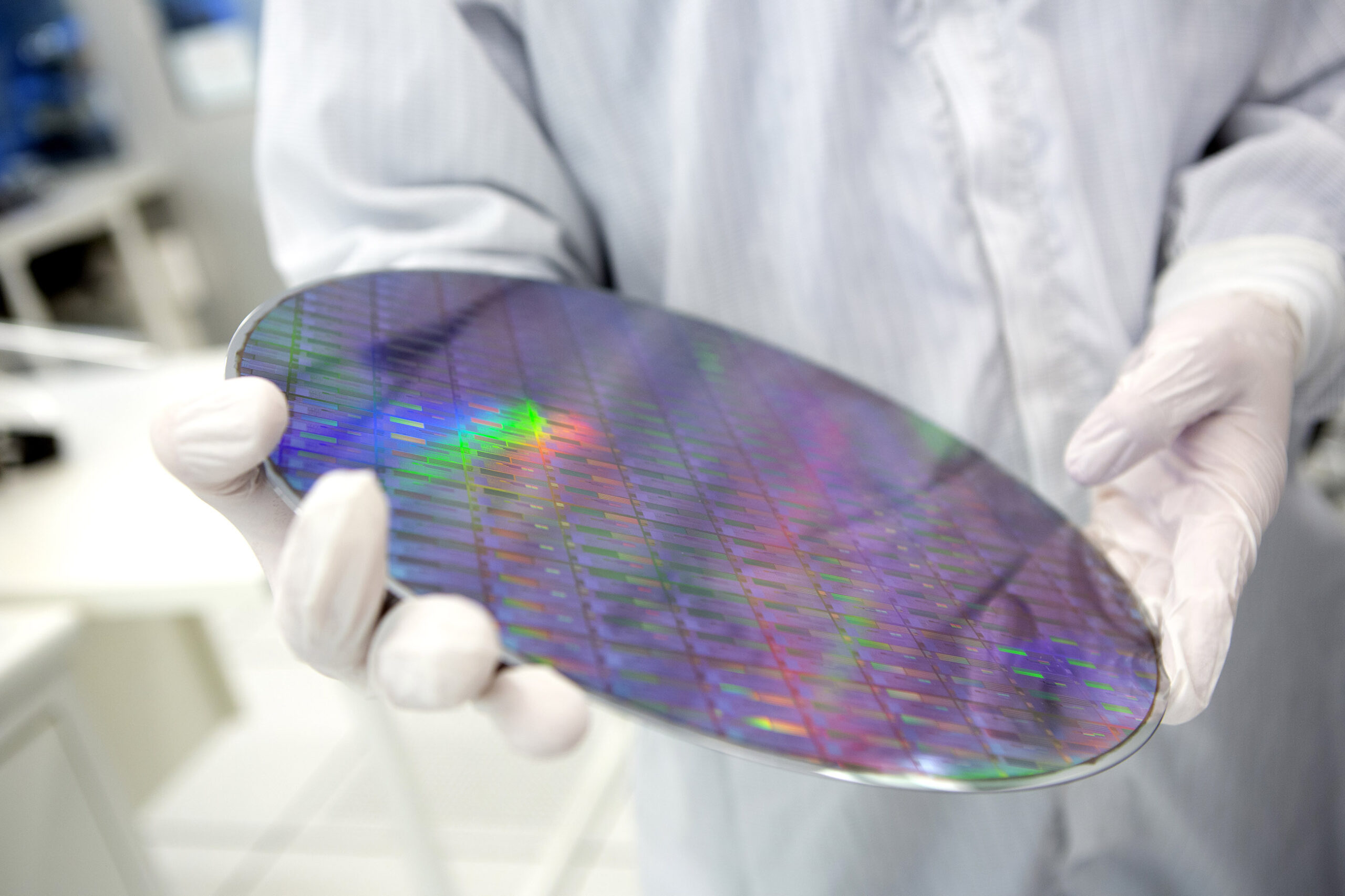
How It Works: Atomic Layer Etching (ALE) Pattern Shaping is a precision etching technique that selectively removes unwanted material from the surface of semiconductor structures. It is particularly effective at addressing surface defects, reducing surface roughness, and mitigating Line Edge Roughness (LER), which are critical challenges in semiconductor manufacturing, especially as feature sizes shrink below 10 nm.
AlixLabs Extreme ALE operates on the principle of sequential, self-limiting chemical reactions that remove atomic layers one at a time. This level of control allows for the precise smoothing of surfaces and edges, which is crucial for maintaining the integrity of nanoscale features. In the context of surface cleaning, ALE can selectively remove contaminants and surface defects without damaging the underlying material, thereby improving the quality of the semiconductor surface.
Reducing Surface Roughness and LER: One of the most significant advantages of ALE is its ability to reduce surface roughness and LER, both of which are major issues after advanced lithography processes like Extreme Ultraviolet (EUV) lithography. At critical dimensions below 10 nm and in densely packed line pitches, even minor surface irregularities can lead to significant performance degradation in semiconductor devices and yield loss.
ALE addresses these issues by smoothing out the rough edges on the sidewalls of features, effectively reducing LER. This is achieved through highly controlled, anisotropic etching, where material is removed uniformly from specific areas without affecting the rest of the structure. By fine-tuning the etching process, ALE can selectively target and smooth out roughness at the atomic level, resulting in cleaner, more precise features with reduced variability.
Applications: ALE Pattern Shaping is highly valuable in the production of advanced semiconductor devices, particularly in processes that require extreme precision, such as those involving EUV lithography. The ability to reduce LER and surface roughness directly translates to better performance, higher yields, and lower defect rates in final semiconductor products. This makes ALE a critical technology for fabricating next-generation chips that power everything from consumer electronics to advanced AI computing systems.
In summary, ALE Pattern Shaping is an essential tool in the semiconductor industry’s toolkit, offering unparalleled precision in surface cleaning and roughness reduction. Its ability to selectively and effectively address LER and surface roughness challenges is vital for the continued advancement of semiconductor technology.