

May 7, 2026
AlixLabs to host APS™ System Launch Event in Eindhoven on June 4
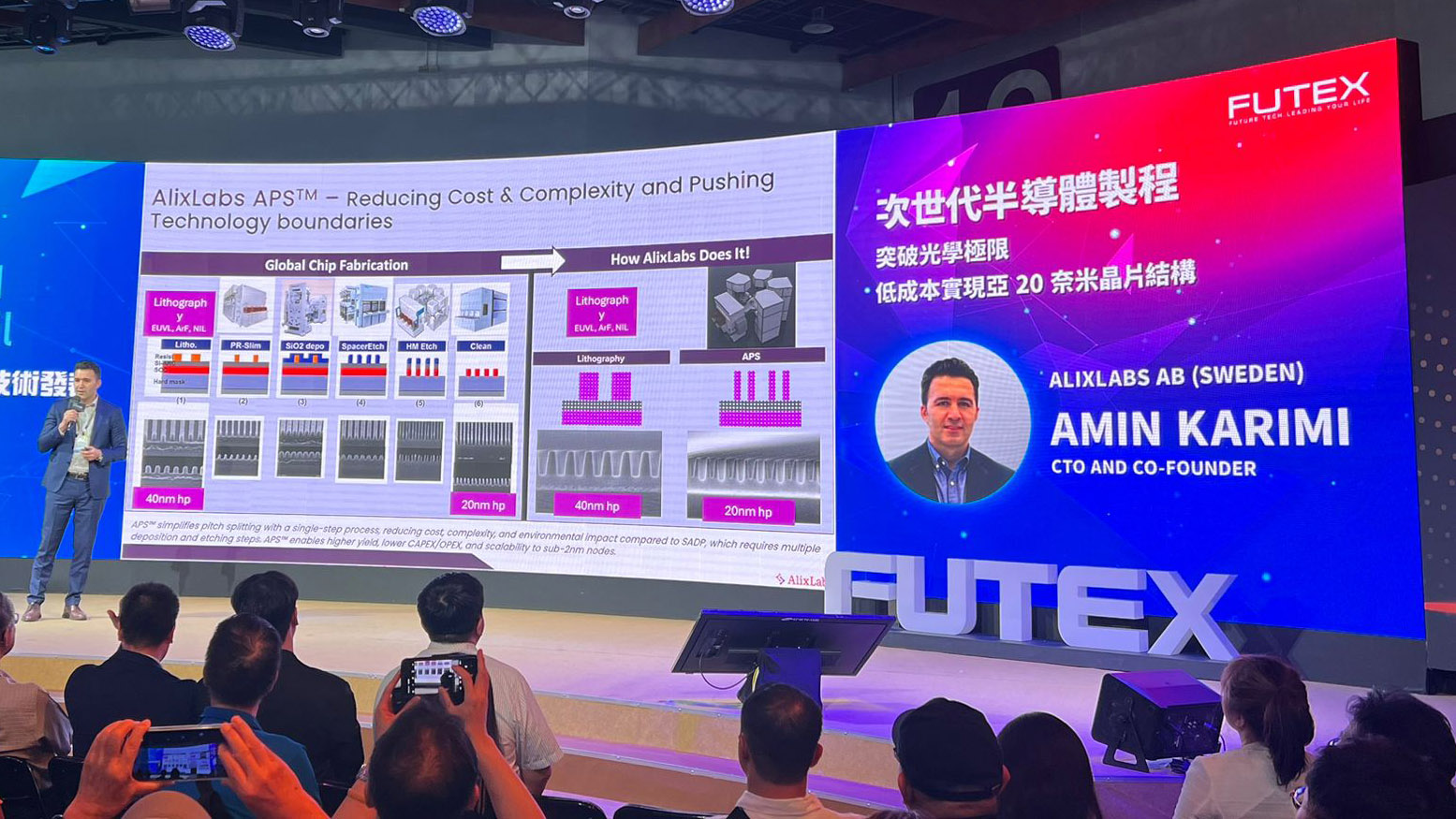
Lund, Sweden – May 7th, 2026 – AlixLabs will host the official launch event for its APS™ (Atomic Pitch Splitting) System, gathering guests from across the semiconductor ecosystem at High Tech Campus Eindhoven in the Netherlands.
The event marks an important milestone in AlixLabs’ transition from technology validation toward industrial deployment, as the company moves to introduce APS™ as a new patterning approach for advanced semiconductor manufacturing.
As advanced semiconductor manufacturing faces increasing challenges related to patterning complexity, process cost and manufacturability, APS™ has been developed to enable advanced pitch division through Atomic Layer Etching-based integration schemes aimed at simplifying multi-patterning flows and reducing process complexity in advanced semiconductor manufacturing.
During the event, AlixLabs will present the APS™ system architecture, recent development progress and the broader industrial implications of the technology, including process integration, manufacturability and future scaling opportunities.
“APS™ has been developed with manufacturability and industrial scalability in mind from the beginning,” said Jonas Sundqvist, CEO and Founder of AlixLabs. “This event represents an important step as we continue expanding our ecosystem engagement and move toward future industrial implementation.”
The APS™ System Launch Event will take place on June 4, 2026 at High Tech Campus Eindhoven in the Netherlands, with registration opening at 15:00 CEST and the main program running from 16:00 to 18:00, followed by networking.
Event details:
Date: June 4, 2026
- Location: High Tech Campus Eindhoven, The Netherlands
- Registration opens: 15:00 CEST
- Main program: 16:00–18:00 CEST
- Networking session: 18:00 onwards
Due to limited venue capacity, registration is required. Additional information and registration details are available here:
About AlixLabs
Established in 2019 in Lund, Sweden, AlixLabs emerged as a spin-off from Lund University with a mission to enable the cost-effective and energy-conscious fabrication of semiconductors, particularly logic and memory components. AlixLabs boasts patented recognition for its groundbreaking APS™ technique, a process that achieves nanostructure division through etching. This method holds approved patents across the USA, Taiwan, and Europe. The APS™ acronym signifies ALE Pitch Splitting, leveraging ALE (Atomic Layer Etching), a plasma-based dry etching cyclic methodology.