
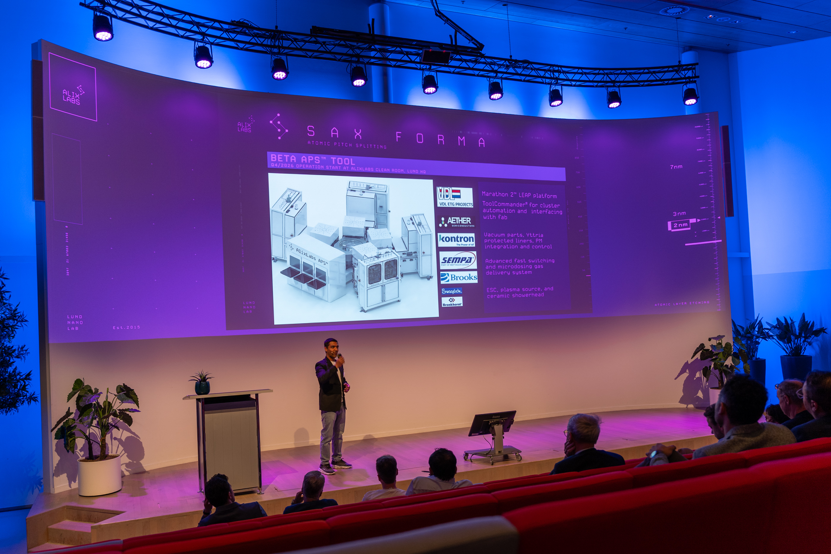
Lund, Sweden – June 23, 2026 – AlixLabs AB, a semiconductor equipment company specializing in advanced etch and patterning technologies, launched Sax Forma, an APS™ System, the company’s first commercially available equipment platform for Atomic Pitch Splitting (APS).
The launch marks AlixLabs’ transition from technology validation toward customer engagement, process integration, and industrial equipment deployment. Sax Forma is designed to bring APS™ into advanced semiconductor manufacturing flows, where continued scaling increasingly depends on reducing patterning complexity.
“With Sax Forma, we are taking APS from validated technology to a commercially available equipment platform,” said Jonas Sundqvist, CEO at AlixLabs. “This is an important step for AlixLabs as we begin deeper customer engagement around how APS can be integrated into existing manufacturing flows and support the industry’s continued scaling roadmap.”
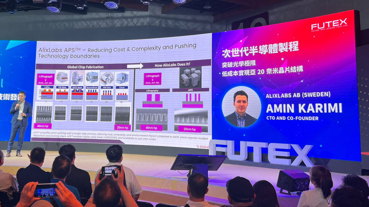
Patterning has become one of the most cost-sensitive and technically demanding areas of advanced chip production, as scaling increasingly requires multi-patterning, additional process loops, and tighter control of critical dimensions, overlay, film thickness, and profile. APS addresses this challenge as a complementary patterning system inserted downstream of established lithography-based process flows, including DUV, EUV, and nanoimprint lithography.
By increasing pattern density without requiring a new lithography platform, APS enables fabs to reduce patterning complexity while preserving existing fab infrastructure and manufacturing investments.
Sax Forma builds on APS demonstrations using industry-relevant silicon, including 300 mm silicon wafers from UMC and Intel FinFET test silicon. On the Intel test silicon, APS reduced the half-pitch from 25 nanometers to 12.5 nanometers, demonstrating performance relevant to geometries associated with the 3-nanometer class. In laboratory settings, AlixLabs has also shown that sequential APS processing can enable further half-pitch reduction, pointing toward future scaling as the industry moves toward 2-nanometer, Ångström-class nodes, and beyond.
Together, these demonstrations support AlixLabs’ core claim: that APS can enable controlled half-pitch refinement in dense, line-based patterning layers without relying on repeated spacer-based process loops.
“APS is designed to complement lithography by adding a controlled pitch-splitting step after the initial pattern has been defined,” said Amin Karimi, CTO at AlixLabs. “The objective is to reduce patterning complexity while preserving compatibility with established process flows. That integration model is central to how we see APS being adopted by semiconductor manufacturers.”
Sax Forma is being industrialized together with VDL ETG Projects, AlixLabs’ partner for system integration and high-tech equipment manufacturing. Building on the collaboration announced earlier this year, VDL ETG Projects is supporting the transition of APS from advanced R&D and process validation into industrial equipment, drawing on its experience in design, engineering, realization, and scale-up from first-of-a-kind systems toward batch manufacturing.
AlixLabs has also built a strong and growing patent portfolio around APS and its equipment platform. The core APS principle is patent protected in key semiconductor markets including the EU, the United States, and Taiwan, while the company expects its process optimization work and hardware innovations to be covered by nine and eleven patent families, respectively, by the end of the year.
Sax Forma enters the market as AlixLabs’ Beta system, intended for customer evaluation, integration work, and validation in production-like environments. As the first commercially available APS equipment platform, it forms the basis for the company’s planned Gamma platform, targeted for 2028.
With Sax Forma, AlixLabs is bringing APS to market as a semiconductor equipment platform that offers a solution to one of the industry’s central scaling challenges: reducing patterning complexity on the path toward the Ångström era.
About AlixLabs
Established in 2019 in Lund, Sweden, AlixLabs emerged as a spin-off from Lund University with a mission to enable the cost-effective and energy-conscious fabrication of semiconductors, particularly logic and memory components. AlixLabs boasts patented recognition for its groundbreaking APS™ technique, a process that achieves nanostructure division through etching. This method holds approved patents across the USA, Taiwan, and Europe. The APS™ acronym signifies ALE Pitch Splitting, leveraging ALE (Atomic Layer Etching), a plasma-based dry etching cyclic methodology.

