The world's only pure-play
Atomic layer etch company
AlixLabs is the world's only pure-play ALE (atomic layer etch) company.
The supply of advanced electronic chips is pivotal for our modern society. As chip complexity increases, so does the cost for both design and manufacture. AlixLabs provides several ALE-based solutions for atomic-level processing that reduce the number of process steps required to manufacture a chip while increasing throughput, with APS™ (Atomic Pitch Splitting) being the flagship process.
All AlixLabs' solutions are designed to slot into existing production workflows, making it more cost-effective than before to advance production to the ångstrom (Å) era. By utilizing APS™, semiconductor companies can drastically reduce consumption of power and water while reducing emissions in leading-edge logic production.
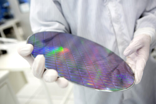
AlixLabs' processes are designed for use on 300 millimeter (12-inch) logic and DRAM silicon wafers, including FinFET and GAAFET (nanowire). They are equally at home in 150 and 200 millimeter wafers for power electronics on materials such as gallium nitride (GaN) and silicon carbide (SiC).
Equipment
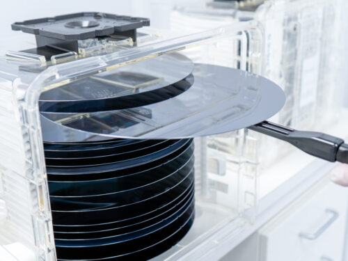
The AlixLabs Sax Forma APS™ chamber is currently in its beta (β) phase, with mass production design being finalized. Demos are being run at AlixLabs HQ Lund, with teams in Lund, Eindhoven and Dresden working on the mass-production gamma (γ) design. For demo opportunities, please contact us.
Our technology
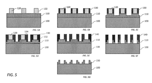
AlixLabs was founded with a mission to make advanced semiconductor manufacturing more cost-effective and energy-conscious. From the outset, the company focused on the APS™ (Atomic Pitch Splitting) process based on Atomic Layer Etching, or ALE, as a way to address one of the industry’s most difficult scaling challenges: creating smaller, denser nanoscale features without adding ever more complex lithography and multi-patterning steps. APS™ grew from this foundation into AlixLabs’ flagship patterning technology, using a plasma-based cyclic dry etching approach to split nanoscale features with atomic-level control.
Since its early development, APS™ has progressed from patented research into a commercially oriented semiconductor equipment platform. The technology has been demonstrated on industry-relevant silicon, including 300 mm wafers and Intel FinFET test structures, where APS™ reduced half-pitch from 25 nm to 12.5 nm. In 2026, AlixLabs advanced the industrialization of APS™ through a partnership with VDL ETG Projects and launched Sax Forma, its first commercially available APS™ system, marking the transition from technology validation toward customer engagement, process integration, and deployment in advanced manufacturing flows.
APS™
Pitch
Splitting
AlixLabs' Atomic Pitch Splitting (APS™) technology is a leading-edge process designed to enhance semiconductor manufacturing. The core of APS™ is the ability to split nanoscale features on semiconductor wafers into even smaller structures using an Extreme form of Atomic Layer Etching (ALE).

How It Works: AlixLabs’ Atomic Pitch Splitting (APS™) technology is a leading-edge process designed to enhance semiconductor manufacturing. The core of APS™ is the ability to split nanoscale features on semiconductor wafers into even smaller structures using an Extreme form of Atomic Layer Etching (ALE) in a simple, economical, and gentle way. This process leverages the unique properties of the sidewalls of nanoscale features, which act as a topographical mask during etching. By utilizing ALE, APS can accurately and efficiently create extremely fine features, with critical dimensions below 10 nm and a tight pitch, on silicon, dielectrics and other materials like gallium phosphide (GaP).
What It Is Good For: APS is highly beneficial in semiconductor fabrication, offering a method to continue scaling down chip components as per Moore’s Law while reducing costs and increasing the throughput. This process is particularly valuable because it allows manufacturers to achieve smaller, more densely packed components without the need for multiple complex lithography steps, which are both expensive and resource-intensive. The APS process thus reduces the capital investment, energy consumption, and the overall environmental impact of semiconductor production.
Applications: APS has broad applications in the semiconductor industry, particularly in the production of advanced logic and memory chips. It is complementary to existing lithography techniques, such as Deep Ultraviolet (DUV) and Extreme Ultraviolet (EUV) lithography and Self-Aligned Double and Quadruple Patterning (SADP and SAQP), but offers a simpler and more cost-effective alternative. This makes APS especially useful in the manufacturing of next-generation integrated circuits and memory devices, where precision at the nanoscale is critical. Furthermore, APS may play a significant role in sustainable semiconductor manufacturing, enabling high-performance chips while minimizing the environmental footprint.
This innovative process by AlixLabs is not only a breakthrough in semiconductor manufacturing but also a strategic step toward more sustainable and cost-effective production, making it a crucial tool for the future of electronics
ALE
Pattern
Shaping
Atomic Layer Etching (ALE) Pattern Shaping is a precision etching technique that selectively removes unwanted material from the surface of semiconductor structures.
How It Works: Atomic Layer Etching (ALE) Pattern Shaping is a precision etching technique that selectively removes unwanted material from the surface of semiconductor structures. It is particularly effective at addressing surface defects, reducing surface roughness, and mitigating Line Edge Roughness (LER), which are critical challenges in semiconductor manufacturing, especially as feature sizes shrink below 10 nm.
AlixLabs Extreme ALE operates on the principle of sequential, self-limiting chemical reactions that remove atomic layers one at a time. This level of control allows for the precise smoothing of surfaces and edges, which is crucial for maintaining the integrity of nanoscale features. In the context of surface cleaning, ALE can selectively remove contaminants and surface defects without damaging the underlying material, thereby improving the quality of the semiconductor surface.
Reducing Surface Roughness and LER: One of the most significant advantages of ALE is its ability to reduce surface roughness and LER, both of which are major issues after advanced lithography processes like Extreme Ultraviolet (EUV) lithography. At critical dimensions below 10 nm and in densely packed line pitches, even minor surface irregularities can lead to significant performance degradation in semiconductor devices and yield loss.
ALE addresses these issues by smoothing out the rough edges on the sidewalls of features, effectively reducing LER. This is achieved through highly controlled, anisotropic etching, where material is removed uniformly from specific areas without affecting the rest of the structure. By fine-tuning the etching process, ALE can selectively target and smooth out roughness at the atomic level, resulting in cleaner, more precise features with reduced variability.
Applications: ALE Pattern Shaping is highly valuable in the production of advanced semiconductor devices, particularly in processes that require extreme precision, such as those involving EUV lithography. The ability to reduce LER and surface roughness directly translates to better performance, higher yields, and lower defect rates in final semiconductor products. This makes ALE a critical technology for fabricating next-generation chips that power everything from consumer electronics to advanced AI computing systems.
In summary, ALE Pattern Shaping is an essential tool in the semiconductor industry’s toolkit, offering unparalleled precision in surface cleaning and roughness reduction. Its ability to selectively and effectively address LER and surface roughness challenges is vital for the continued advancement of semiconductor technology.
ALE
Surface
Smoothening
Atomic Layer Etching (ALE) Surface Smoothening is an advanced etching technique developed by AlixLabs to enhance the surface quality of semiconductor materials, particularly GaN (Gallium Nitride) and SiC (Silicon Carbide).
How It Works: Atomic Layer Etching (ALE) Surface Smoothening is an advanced etching technique developed by AlixLabs to enhance the surface quality of semiconductor materials, particularly GaN (Gallium Nitride) and SiC (Silicon Carbide). This technique involves removing material at the atomic scale with high precision, allowing for controlled smoothing of surfaces. AlixLabs Extreme ALE operates by leveraging self-limiting chemical reactions and physical plasma generated ion bombardment that can remove only a single atomic layer at a time or even just surface defects.
What It Is Good For: ALE Surface Smoothening is particularly beneficial for improving the performance and reliability of GaN and SiC-based transistors, which are commonly used in high-power and high-temperature applications, such as power electronics and RF (radio frequency) devices. By precisely smoothing the surfaces and reducing roughness, ALE enhances the electrical properties of these transistors, leading to lower resistive losses, better thermal management, and more consistent device performance. The ability to control the etching process without damaging the transistor channel improves the yield and performance of the transistors.
Applications: The primary applications of ALE Surface Smoothening are in the semiconductor industry, particularly in the fabrication of advanced GaN and SiC transistors used in power converters, electric vehicles, telecommunications infrastructure, and RF communication systems. The technology is crucial for manufacturing next-generation electronic components that require high efficiency, reliability, and performance in challenging environments. By improving the surface quality of these materials, ALE Surface Smoothening enables the production of semiconductors that can operate at higher voltages and temperatures, making it a key technology for the future of power electronics and other high-performance applications.