

August 6, 2026
AlixLabs Expands Footprint at RISE ProNano in Lund by 400 Square Meters
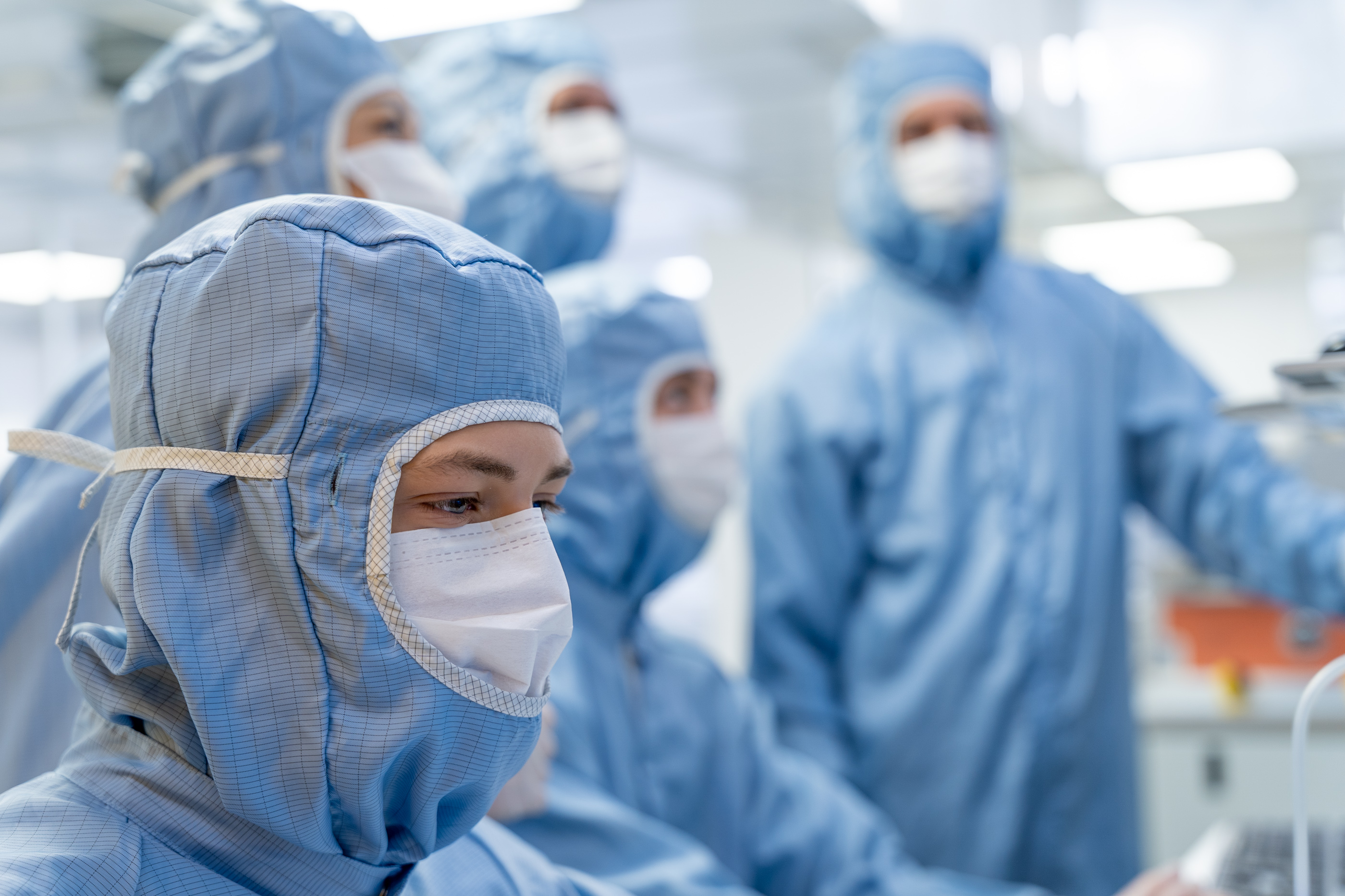
New capacity supports continued commercialization of APS™ technology and expanded beta testing for semiconductor customers.
LUND, Sweden — August 6, 2026 — AlixLabs AB, a Swedish semiconductor technology company pioneering Atomic Pitch Splitting, APS™, today announced that it is expanding its cleanroom space at the Lund-based RISE ProNano lab by 400 square meters.
The expansion is part of AlixLabs’ continuous growth plan as the company advances from technology development toward commercialization. The additional cleanroom capacity will provide AlixLabs with more space to install, qualify and operate equipment for customer-facing beta activities, including semiconductor wafer processing and process validation for leading semiconductor clients.
A central part of the expansion is preparation for the company’s APS Beta platform, which is expected to become operational in the second half of 2026. The platform will allow AlixLabs to run more extensive beta tests with semiconductor customers and support the transition of APS™ from pilot-scale development toward commercial manufacturing use cases.
“Expanding our cleanroom footprint at RISE ProNano is a significant step in our commercialization roadmap,” said Jonas Sundqvist, CEO of AlixLabs “The additional 400 square meters give us the infrastructure needed to scale our beta activities, support customer evaluations and demonstrate the value of APS™ in a production-relevant environment.”
AlixLabs’ APS™ technology is designed to enable advanced semiconductor patterning through a fast atomic layer etching (ALE) process, creating extremely small and precise structures while reducing process complexity. By expanding its cleanroom capacity, the company is strengthening its ability to support semiconductor customers as they evaluate new approaches to future chip manufacturing.
The expansion also reinforces AlixLabs’ long-term presence in Lund’s semiconductor ecosystem. Based at RISE ProNano, AlixLabs benefits from access to advanced infrastructure, process expertise and a collaborative environment designed to support the scaling of next-generation semiconductor technologies.
“This expansion is not only about more space,” added Sundqvist. “It is about building the operational foundation required for commercialization. With the APS™ Beta platform coming online later this year, we are creating the capacity needed to work more closely with customers and accelerate the path toward industrial adoption.”
About AlixLabs
Established in 2019 in Lund, Sweden, AlixLabs emerged as a spin-off from Lund University with a mission to enable the cost-effective and energy-conscious fabrication of semiconductors, particularly logic and memory components. AlixLabs boasts patented recognition for its groundbreaking APS™ technique, a process that achieves nanostructure division through etching. This method holds approved patents across the USA, Taiwan, and Europe. The APS™ acronym signifies Atomic Pitch Splitting, leveraging ALE (Atomic Layer Etching), a plasma-based dry etching cyclic methodology. For more details, please visit www.alixlabs.com.