May 6, 2025AlixLabs Secures Notice of Allowance for US Patent for Innovative Semiconductor Manufacturing TechnologySwedish semiconductor startup’s APS™ patent portfolio continues to grow with new U.S. patent, marking the company’s 10th pending global patent.
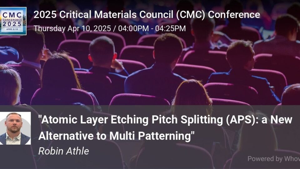
April 10, 2025AlixLabs to Demonstrate APS™ on 300-millimeter UMC wafers at the 2025 CMC ConferenceAtomic Layer Etching Pitch Splitting (APS) proven on more industry-leading wafers, doubling fin density and proving flexibility without EUV.
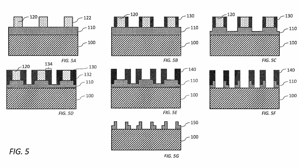
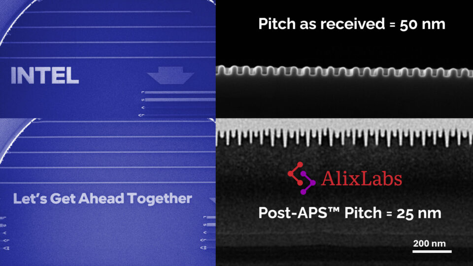
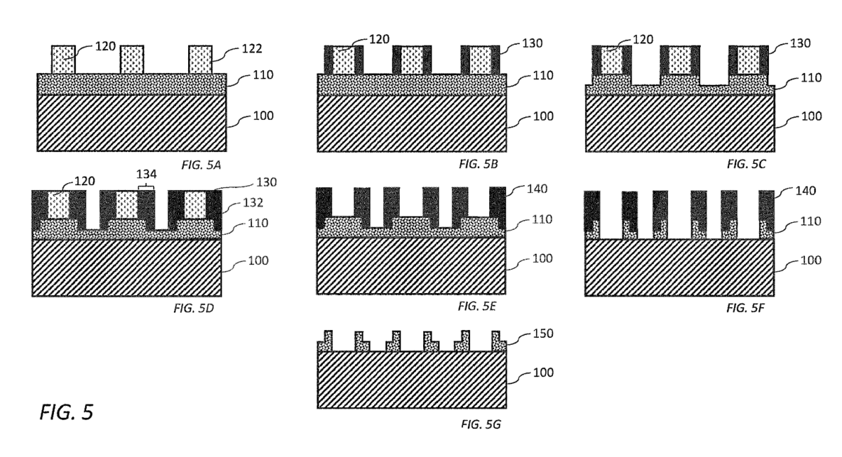
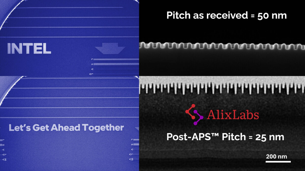
February 7, 2025AlixLabs to Showcase Latest APS™ Findings at SPIE Advanced Lithography + PatterningSwedish semiconductor startup to demonstrate 3-nanometer class FinFET structures made with APS™ on Intel Silicon at trade show.
February 4, 2025AlixLabs Announces Research Collaboration with Linköping UniversitySwedish semiconductor startup and leading Swedish university to explore joint research in gallium nitride (GaN) and indium nitride (InN).


