


August 28, 2026
AlixLabs Sax Forma Beta Chamber Enters Final Assembly at VDL Projects
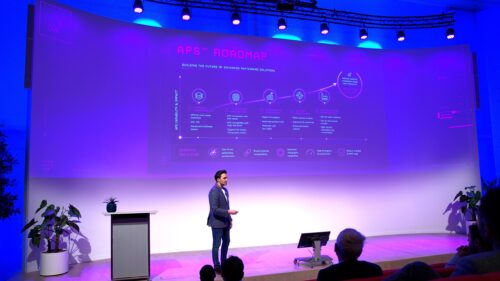
Lund, Sweden – August 28, 2026 – AlixLabs AB, a semiconductor equipment company specializing in advanced etch and patterning technologies, today announced that the assembly of its first Sax Forma Beta tool for Atomic Pitch Splitting, APS™, has commenced at VDL Projects, The Netherlands.
This milestone keeps AlixLabs on track to install the Sax Forma Beta tool in its own cleanroom by the end of 2026, enabling beta testing of APS™ for customers and partners.
The second Beta tool will enter the assembly phase as well before the end of this year. These developments are part of AlixLabs’ continued transition from technology validation toward deeper customer engagement, process integration, and industrial equipment deployment. Following the launch of Sax Forma, AlixLabs’ first commercially available APS™ System, the Sax Forma Beta tools represent the next step in preparing APS™ for evaluation in mass production environments.
“Starting the assembly of the Sax Forma Beta tool is an important commercial milestone for AlixLabs,” said Jonas Sundqvist, CEO at AlixLabs. “It means we are moving from demonstrating the core APS capability toward beta testing with customers where we can return contamination free wafers to the customer pilot lines and actual fabs. This is critical for process integration, showcasing manufacturing value, and the role APS can play in reducing patterning complexity and cutting cost for advanced semiconductor manufacturing.”
APS™ is designed as a complementary patterning system inserted downstream of established lithography-based process flows, including DUV, EUV, and nanoimprint lithography (NIL). By enabling controlled pitch splitting after the initial pattern has been defined, APS™ can increase pattern density without subsequent passes of lithography.
The Sax Forma Beta tools are being industrialized together with industry heavyweight VDL Projects, AlixLabs’ partner for system integration and high-tech equipment manufacturing. VDL Projects is supporting the transition of APS™ from advanced R&D and process validation into industrial equipment, drawing on its experience in design, engineering, realization, and scale-up of first-of-a-kind systems.
“Completing the design and engineering of the first-of-a-kind APS™ equipment on schedule has been a tremendous challenge,” said Sorin Stan, Senior Director for Emerging Technologies at VDL Projects. “We did not experience a single week of delay, which preserved the overall planning for the realization phase. The manufacturing and procurement of parts, the assembly currently underway, and the testing before shipment have been planned with half-day accuracy. This showcases our extensive experience in enabling ambitious, accelerated growth of both small and large companies at times when novel equipment is paramount to their success.”
Once installed in AlixLabs’ cleanroom, the Sax Forma Beta tools will support automated production-like APS™ demonstrations for customer evaluation, integration work, and validation on industry-relevant silicon design for logic and memory products at the advanced technology nodes. The beta testing will help semiconductor manufacturers assess how APS™ can be integrated into existing manufacturing flows while preserving fab infrastructure and reducing patterning complexity.
The Sax Forma Beta tools also support AlixLabs’ longer-term equipment roadmap, with additional deliveries scheduled for customers in 2027. The Beta tools also form an important step toward the company’s planned final high-volume manufacturing (HVM) Gamma platform targeted for 2028.
With the Sax Forma Beta tools now in full assembly, AlixLabs continues to advance APS™ toward commercial adoption as a semiconductor equipment platform for the Ångström era.
About AlixLabs
Established in 2019 in Lund, Sweden, AlixLabs emerged as a spin-off from Lund University with a mission to enable the cost-effective and energy-conscious fabrication of semiconductors, particularly logic and memory components. AlixLabs boasts patented recognition for its groundbreaking APS™ technique, a process that achieves nanostructure division through etching. This method holds approved patents across the USA, Taiwan, and Europe. The APS™ acronym signifies Atomic Pitch Splitting, leveraging ALE (Atomic Layer Etching), a plasma-based dry etching cyclic methodology. For more details, please visit www.alixlabs.com.
About VDL Projects
As part of VDL Groep of The Netherlands, VDL Projects has a proven track record in supporting innovative companies in the transition from the feasibility to the design, engineering, and realization of their equipment. With all needed expertise under one roof, VDL Projects scales up the equipment manufacturing from first-of-a-kind units to batch manufacturing, and further to turnkey realization of complex production lines. VDL Groep is an industrial conglomerate headquartered in Eindhoven, The Netherlands. It was founded in 1953 and consists currently of more than 100 specialized companies employing together more than 14,000 employees in 20 countries and operating in several industrial sectors. For more details, please visit https://www.vdlgroep.com/en.
August 6, 2026
AlixLabs Expands Footprint at RISE ProNano in Lund by 400 Square Meters

New capacity supports continued commercialization of APS™ technology and expanded beta testing for semiconductor customers.
LUND, Sweden — August 6, 2026 — AlixLabs AB, a Swedish semiconductor technology company pioneering Atomic Pitch Splitting, APS™, today announced that it is expanding its cleanroom space at the Lund-based RISE ProNano lab by 400 square meters.
The expansion is part of AlixLabs’ continuous growth plan as the company advances from technology development toward commercialization. The additional cleanroom capacity will provide AlixLabs with more space to install, qualify and operate equipment for customer-facing beta activities, including semiconductor wafer processing and process validation for leading semiconductor clients.
A central part of the expansion is preparation for the company’s APS Beta platform, which is expected to become operational in the second half of 2026. The platform will allow AlixLabs to run more extensive beta tests with semiconductor customers and support the transition of APS™ from pilot-scale development toward commercial manufacturing use cases.
“Expanding our cleanroom footprint at RISE ProNano is a significant step in our commercialization roadmap,” said Jonas Sundqvist, CEO of AlixLabs “The additional 400 square meters give us the infrastructure needed to scale our beta activities, support customer evaluations and demonstrate the value of APS™ in a production-relevant environment.”
AlixLabs’ APS™ technology is designed to enable advanced semiconductor patterning through a fast atomic layer etching (ALE) process, creating extremely small and precise structures while reducing process complexity. By expanding its cleanroom capacity, the company is strengthening its ability to support semiconductor customers as they evaluate new approaches to future chip manufacturing.
The expansion also reinforces AlixLabs’ long-term presence in Lund’s semiconductor ecosystem. Based at RISE ProNano, AlixLabs benefits from access to advanced infrastructure, process expertise and a collaborative environment designed to support the scaling of next-generation semiconductor technologies.
“This expansion is not only about more space,” added Sundqvist. “It is about building the operational foundation required for commercialization. With the APS™ Beta platform coming online later this year, we are creating the capacity needed to work more closely with customers and accelerate the path toward industrial adoption.”
About AlixLabs
Established in 2019 in Lund, Sweden, AlixLabs emerged as a spin-off from Lund University with a mission to enable the cost-effective and energy-conscious fabrication of semiconductors, particularly logic and memory components. AlixLabs boasts patented recognition for its groundbreaking APS™ technique, a process that achieves nanostructure division through etching. This method holds approved patents across the USA, Taiwan, and Europe. The APS™ acronym signifies Atomic Pitch Splitting, leveraging ALE (Atomic Layer Etching), a plasma-based dry etching cyclic methodology. For more details, please visit www.alixlabs.com.
June 23, 2026
AlixLabs launches Sax Forma for the Ångström era
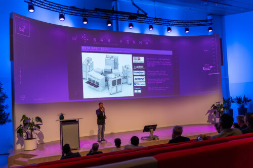
Lund, Sweden – June 23, 2026 – AlixLabs AB, a semiconductor equipment company specializing in advanced etch and patterning technologies, launched Sax Forma, an APS™ System, the company’s first commercially available equipment platform for Atomic Pitch Splitting (APS).
The launch marks AlixLabs’ transition from technology validation toward customer engagement, process integration, and industrial equipment deployment. Sax Forma is designed to bring APS™ into advanced semiconductor manufacturing flows, where continued scaling increasingly depends on reducing patterning complexity.
“With Sax Forma, we are taking APS from validated technology to a commercially available equipment platform,” said Jonas Sundqvist, CEO at AlixLabs. “This is an important step for AlixLabs as we begin deeper customer engagement around how APS can be integrated into existing manufacturing flows and support the industry’s continued scaling roadmap.”
Patterning has become one of the most cost-sensitive and technically demanding areas of advanced chip production, as scaling increasingly requires multi-patterning, additional process loops, and tighter control of critical dimensions, overlay, film thickness, and profile. APS addresses this challenge as a complementary patterning system inserted downstream of established lithography-based process flows, including DUV, EUV, and nanoimprint lithography.
By increasing pattern density without requiring a new lithography platform, APS enables fabs to reduce patterning complexity while preserving existing fab infrastructure and manufacturing investments.
Sax Forma builds on APS demonstrations using industry-relevant silicon, including 300 mm silicon wafers from UMC and Intel FinFET test silicon. On the Intel test silicon, APS reduced the half-pitch from 25 nanometers to 12.5 nanometers, demonstrating performance relevant to geometries associated with the 3-nanometer class. In laboratory settings, AlixLabs has also shown that sequential APS processing can enable further half-pitch reduction, pointing toward future scaling as the industry moves toward 2-nanometer, Ångström-class nodes, and beyond.
Together, these demonstrations support AlixLabs’ core claim: that APS can enable controlled half-pitch refinement in dense, line-based patterning layers without relying on repeated spacer-based process loops.
“APS is designed to complement lithography by adding a controlled pitch-splitting step after the initial pattern has been defined,” said Amin Karimi, CTO at AlixLabs. “The objective is to reduce patterning complexity while preserving compatibility with established process flows. That integration model is central to how we see APS being adopted by semiconductor manufacturers.”
Sax Forma is being industrialized together with VDL ETG Projects, AlixLabs’ partner for system integration and high-tech equipment manufacturing. Building on the collaboration announced earlier this year, VDL ETG Projects is supporting the transition of APS from advanced R&D and process validation into industrial equipment, drawing on its experience in design, engineering, realization, and scale-up from first-of-a-kind systems toward batch manufacturing.
AlixLabs has also built a strong and growing patent portfolio around APS and its equipment platform. The core APS principle is patent protected in key semiconductor markets including the EU, the United States, and Taiwan, while the company expects its process optimization work and hardware innovations to be covered by nine and eleven patent families, respectively, by the end of the year.
Sax Forma enters the market as AlixLabs’ Beta system, intended for customer evaluation, integration work, and validation in production-like environments. As the first commercially available APS equipment platform, it forms the basis for the company’s planned Gamma platform, targeted for 2028.
With Sax Forma, AlixLabs is bringing APS to market as a semiconductor equipment platform that offers a solution to one of the industry’s central scaling challenges: reducing patterning complexity on the path toward the Ångström era.
About AlixLabs
Established in 2019 in Lund, Sweden, AlixLabs emerged as a spin-off from Lund University with a mission to enable the cost-effective and energy-conscious fabrication of semiconductors, particularly logic and memory components. AlixLabs boasts patented recognition for its groundbreaking APS™ technique, a process that achieves nanostructure division through etching. This method holds approved patents across the USA, Taiwan, and Europe. The APS™ acronym signifies ALE Pitch Splitting, leveraging ALE (Atomic Layer Etching), a plasma-based dry etching cyclic methodology.
May 7, 2026
AlixLabs to host APS™ System Launch Event in Eindhoven on June 4
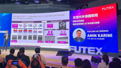
Lund, Sweden – May 7th, 2026 – AlixLabs will host the official launch event for its APS™ (Atomic Pitch Splitting) System, gathering guests from across the semiconductor ecosystem at High Tech Campus Eindhoven in the Netherlands.
The event marks an important milestone in AlixLabs’ transition from technology validation toward industrial deployment, as the company moves to introduce APS™ as a new patterning approach for advanced semiconductor manufacturing.
As advanced semiconductor manufacturing faces increasing challenges related to patterning complexity, process cost and manufacturability, APS™ has been developed to enable advanced pitch division through Atomic Layer Etching-based integration schemes aimed at simplifying multi-patterning flows and reducing process complexity in advanced semiconductor manufacturing.
During the event, AlixLabs will present the APS™ system architecture, recent development progress and the broader industrial implications of the technology, including process integration, manufacturability and future scaling opportunities.
“APS™ has been developed with manufacturability and industrial scalability in mind from the beginning,” said Jonas Sundqvist, CEO and Founder of AlixLabs. “This event represents an important step as we continue expanding our ecosystem engagement and move toward future industrial implementation.”
The APS™ System Launch Event will take place on June 4, 2026 at High Tech Campus Eindhoven in the Netherlands, with registration opening at 15:00 CEST and the main program running from 16:00 to 18:00, followed by networking.
Event details:
Date: June 4, 2026
- Location: High Tech Campus Eindhoven, The Netherlands
- Registration opens: 15:00 CEST
- Main program: 16:00–18:00 CEST
- Networking session: 18:00 onwards
Due to limited venue capacity, registration is required. Additional information and registration details are available here:
About AlixLabs
Established in 2019 in Lund, Sweden, AlixLabs emerged as a spin-off from Lund University with a mission to enable the cost-effective and energy-conscious fabrication of semiconductors, particularly logic and memory components. AlixLabs boasts patented recognition for its groundbreaking APS™ technique, a process that achieves nanostructure division through etching. This method holds approved patents across the USA, Taiwan, and Europe. The APS™ acronym signifies ALE Pitch Splitting, leveraging ALE (Atomic Layer Etching), a plasma-based dry etching cyclic methodology.
April 14, 2026
AlixLabs Closes 15 M EUR Series A with Strategic Investment from Stephen Industries

Lund, Sweden – April 14th, 2026 – AlixLabs, a pioneer in Atomic Layer Etching (ALE) technology for next-generation semiconductor manufacturing, today announced that it closed its 15 million euro Series A in the first quarter of 2026 following a strategic investment from Stephen Industries, a Finnish investment company with a strong track record in scaling advanced technology ventures.
In November 2025, AlixLabs announced that Global Brain and key institutional investors had subscribed to its Series A to the tune of 14,1 million euro, with the difference to the 15 million total remaining open until the first quarter of 2026.
The investment marks a strategic milestone for AlixLabs as it continues to develop its proprietary ALE solutions with especially its flagship APS™ (Atomic Pitch Splitting) technology aimed at enabling more precise, efficient, and cost-effective semiconductor fabrication.
A key dimension of the partnership is the involvement of Kustaa Poutiainen of Stephen Industries, whose experience in building and scaling deep-tech companies brings significant strategic value. Poutiainen previously played a central role in the growth of Picosun, a Nordic Atomic Layer Deposition (ALD) company that became a global leader in its field. Given the close technological relationship between ALD and ALE, this track record is particularly relevant to AlixLabs’ mission.
“Stephen Industries brings deep industrial expertise and a proven ability to scale companies in adjacent technology domains,” said Jonas Sundqvist, CEO of AlixLabs. “Kustaa’s experience with Picosun is especially valuable as we move from development toward broader commercialization of our APS™ platform.”
Atomic Layer Etching is widely seen as a critical enabler for future semiconductor nodes, complementing ALD processes by allowing atomic-scale precision in material removal. As device architectures become increasingly complex, ALE is expected to play a central role in manufacturing.
“AlixLabs operates in a highly promising space within semiconductor process technology,” said Kustaa Poutiainen, Chairman and President of Stephen Industries. “Having seen firsthand how ALD evolved from a niche innovation to a critical industry standard, I see strong parallels with ALE. AlixLabs has the potential to follow a similar trajectory.”
The new funding will be used to accelerate product development, expand technical capabilities, and strengthen partnerships with semiconductor manufacturers.
This investment reinforces AlixLabs’ position as a key innovator in the European semiconductor ecosystem and supports its ambition to become a global leader in Atomic Layer Etching.
Older articles
August 28, 2025
AlixLabs Chosen as a Winner in IC Taiwan Grand Challenge

Lund, Sweden – August 28th, 2025 – AlixLabs has been selected as a winning entrant from the third batch of the IC Taiwan Grand Challenge, an international competition that recognizes groundbreaking innovations in semiconductor and related technologies.
Out of a highly competitive global field, AlixLabs was selected for its Atomic Layer Etch Pitch Splitting (APS™) technology – a breakthrough equipment solution designed to enable advanced semiconductor manufacturing. This recognition highlights AlixLabs’ role in addressing critical challenges in next-generation chip production, particularly as the industry pushes toward ever-smaller nodes, increasing the need for more energy-efficient solutions.
The IC Taiwan Grand Challenge, organized by Taiwan’s National Science and Technology Council (NSTC), brings together leading technology companies and research-driven startups from around the world. The program is designed to foster international collaboration, accelerate cutting-edge innovation, and strengthen the global semiconductor ecosystem.
“We are honored that the NSTC and the IC Taiwan Grand Challenge jury has deemed AlixLabs and APS™ a winning entry from the pool of 150 participants. This recognition of our technology underlines our belief that it can transform leading-edge semiconductor manufacturing and there is no better place to do this than in Taiwan,” comments Amin Karimi, COO and R&D Manager at AlixLabs.
AlixLabs joins a distinguished group of finalists from across the United States, Taiwan, South Korea and Denmark, with the final ceremony held on October 18th 13:00–14:30 (CST, GMT+8) at The Taiwan Innotech Expo.
August 11, 2025
AlixLabs Named to EE Times Silicon 100 for Third Year in a Row

For the third consecutive year, AlixLabs has been recognized on the EE Times Silicon 100 list, cementing our place among the world’s most innovative semiconductor startups. We’re proud to represent Sweden as the sole company featured in this year’s edition.
The Silicon 100 is an annual ranking spotlighting breakthrough companies that are driving the future of chip technology. Notably, Europe’s presence on the list continues to grow — with 29 startups included in 2025, up from 23 in 2024 and 18 in 2023.
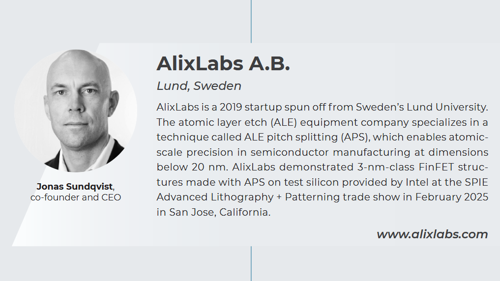
“This recognition is a reflection of our team’s dedication to innovation and our mission to push semiconductor manufacturing into new frontiers,” said Jonas Sundqvist, CEO at AlixLabs. “Being part of the Silicon 100 yet again is both an honor and a responsibility to keep challenging the limits of what’s possible.”
You can explore the full Silicon 100 list on EE Times to see the global community of innovators shaping the semiconductor industry’s future.
August 7, 2025
AlixLabs and NSS Water Partner to Revolutionize Sustainable Ultrapure Water Management in Semiconductor Manufacturing
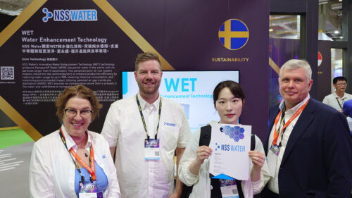
Co-financed by ASCENT+ and leveraging Fraunhofer IPMS metrology for advanced defect control, the collaboration aims to cut costs, reduce environmental footprint, and enhance water recycling.
Stockholm, Sweden – August 7th, 2025 – AlixLabs and NSS Water are pleased to announce a strategic collaboration to develop sustainable and cost-effective ultrapure water (UPW) management solutions for chip production. Amid rising concerns over the semiconductor industry’s ever-increasing water consumption and regulatory pressure to reduce environmental impact, the two Swedish companies will team up to address this challenge.
The project value is approximately 28,000 euros, with funding coming from the European Union’s ASCENT+ program and is overseen by Fraunhofer IPMS (Institute for Photonic Microsystems.)
By integrating Fraunhofer IPMS’s state-of-the-art metrology expertise in advanced defect and contamination control, the partnership aims to improve and elevate water recycling methods, reduce chemical usage, and optimize overall process efficiency – paving the way for smarter water solutions in a water-constrained future.
According to industry data, the semiconductor sector has experienced a 20–30% increase in water consumption in recent years, with the average chip manufacturing facility using up to 10 million gallons of UPW daily – an amount equivalent to the daily water needs of a city of 300,000 people. Producing UPW traditionally comes at a significant cost: it can be 60 to 350 times more expensive than drinking water due to the intensive energy and chemical processes required. This is the challenge NSS Water addresses with its nano-pure water (NPW).
The semiconductor industry’s water consumption is projected to keep increasing due to more advanced plants with higher consumption coming online in the coming years. Additionally, 40% of chip production facilities are projected to be located in high-water-risk areas by 2030, meaning the need for data-driven, circular water strategies has never been more critical.
“Water is the lifeblood of our planet and the backbone of the semiconductor industry,” says Reza Jafari Jam, Research Director at AlixLabs. “This collaborative research on water conservation not only safeguards a finite resource but fuels innovation, ensuring sustainable growth and technological advancement. We push the semiconductor industry to be more sustainable with our APS™ patterning process technology and our collaboration with NSS Water will further solidify our position as an enabler tomorrow’s green semiconductor production.”
“We are happy to expand our collaboration with AlixLabs and Fraunhofer,” says Björn Holmström, CEO at NSS Water. “The importance of advanced metrology will help us provide a platform that improves the water infrastructure used by AlixLabs and other advanced semiconductor players. With this project, we get to benchmark our NPW on 300-millimeter wafers as well as have the wafers cleaned with NPW by Fraunhofer.”
Through this partnership, AlixLabs and NSS Water are combining their respective strengths in innovative water treatment, advanced analytics, and semiconductor manufacturing know-how to develop solutions that significantly reduce water usage, lower operational costs, and bolster sustainability. Fraunhofer IPMS’s involvement ensures precise contamination and defect control, further enhancing the effectiveness of the recycling and purification processes.
Co-financed by the European Nanoelectronics Access program ASCENT+, which provides a direct gateway to Europe’s global-scale Nanoelectronics Research Infrastructure, granting researchers, SMEs, and PhD candidates access to state-of-the-art capabilities. The project is an important step in positioning AlixLabs, NSS Water and the European Union at the forefront of sustainable semiconductor manufacturing innovations.
About AlixLabs
Established in 2019 in Lund, Sweden, AlixLabs emerged as a spin-off from Lund University with a mission to enable the cost-effective and energy-conscious fabrication of semiconductors, particularly logic and memory components. AlixLabs boasts patented recognition for its groundbreaking APS™ technique, a process that achieves nanostructure division through etching. This method holds approved patents across the USA, Taiwan, and Europe. The APS™ acronym signifies ALE Pitch Splitting, leveraging ALE (Atomic Layer Etching), a plasma-based dry etching cyclic methodology. For more details, please visit www.alixlabs.com
June 28, 2025
AlixLabs Named Semi-Finalist in SEMI S3 Program for Sustainable Semiconductor Innovation
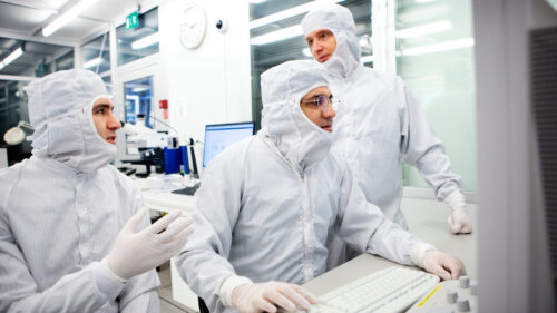
Efforts with APS™ recognized for driving sustainable leading-edge semiconductor production.
Lund, Sweden – June 28, 2025 — AlixLabs, an innovative semiconductor equipment startup based in Lund, Sweden, has been named a semi-finalist in the prestigious 2025 SEMI Startups for Sustainable Semiconductors (S3) program. Now in its fourth year, the S3 program has drawn global attention for highlighting early-stage companies that are making groundbreaking contributions to sustainability in the semiconductor industry.
This year’s competition reached a new milestone, receiving a record 145 applications from startups around the world. AlixLabs is one of only 35 companies selected to advance to the semi-final round — a significant endorsement of its innovative Atomic Layer Pitch Splitting (APS™) technology.
APS™ is a patented process that addresses one of the semiconductor industry’s most pressing challenges: how to continue scaling transistor architectures affordably and sustainably as traditional lithography methods become increasingly complex and costly. By doubling pattern density at half the cost and integrating seamlessly into existing fabrication lines, APS™ enables more efficient manufacturing without relying on the latest and most expensive lithography tools.
Crucially, APS™ also contributes to reducing the environmental impact of semiconductor production — a sector known for its intensive energy and resource use. The technology supports energy-efficient scaling while lowering overall manufacturing costs, aligning closely with the SEMI S3 program’s mission to accelerate eco-friendly innovation in chipmaking.
“We are proud and honored to be recognized by SEMI and the S3 Committee, led by Applied Materials,” said Dr. Jonas Sundqvist, CEO of AlixLabs. “Our inclusion as a semi-finalist underscores the real-world impact and potential of our APS™ technology in advancing the global transition to more sustainable semiconductor manufacturing.”
As a semi-finalist, AlixLabs will participate in the S3 virtual pitch event scheduled for July 31 and August 1, where selected startups will present their solutions to an expert panel of judges, industry leaders, and potential investors.
The SEMI S3 program is organized by SEMI, the global industry association serving the electronics manufacturing and design supply chain. It aims to foster innovative startups that are pioneering technologies to improve the environmental sustainability of semiconductor production.
For more information about the SEMI S3 program, visit semi.org. To learn more about AlixLabs and its APS™ technology, visit alixlabs.com.
June 3, 2025
AlixLabs appoints Per-Anders Eriksson as General Manager
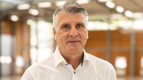
New General Manager to drive the company’s next growth phase at a time of crucial company expansion.
Lund, Sweden – June 3rd, 2025 — AlixLabs, a pioneering Swedish semiconductor startup known for its disruptive patterning technologies, proudly announces the appointment of Per-Anders Eriksson as its new General Manager, effective June 1, 2025.
With over three decades of leadership experience in the global semiconductor and high-tech industries, Eriksson brings strategic insight and operational expertise to AlixLabs at a time of rapid growth and international expansion. His proven track record in scaling technology ventures, coupled with deep domain knowledge, will be instrumental as the company advances its breakthrough Atomic Layer Etch Pitch Splitting (APS™) technology towards commercialization.
Prior to joining AlixLabs, Eriksson held senior leadership roles at several multinational companies, where he successfully led business development, product strategy, and global operations. His international experience and ability to lead high-performing teams make him well-suited to drive AlixLabs’ next phase of growth.
“I’m thrilled to join AlixLabs and contribute to a team that’s redefining the future of semiconductor manufacturing,” said Per-Anders Eriksson. “The company’s innovative approach to patterning opens up significant opportunities for more cost-efficient and scalable chip production. I look forward to working with the team to deliver on its bold vision.”
“We are excited to welcome Per-Anders to AlixLabs,” said Jonas Sundqvist, CEO of AlixLabs. “His leadership, strategic acumen, and industry experience will be invaluable as we transition from R&D to commercial engagement with global partners. Not only will Eriksson boost our work with APS™ for leading edge logic and memory production, his experience in silicon carbide will also be an asset for our power electronics applications as we look to support EU’s green transition with our technologies.”
Founded in Lund, Sweden, AlixLabs is at the forefront of enabling next-generation semiconductor manufacturing through its patented APS™ technology, which allows for reduced complexity and cost in advanced node fabrication.
May 6, 2025
AlixLabs Secures Notice of Allowance for US Patent for Innovative Semiconductor Manufacturing Technology
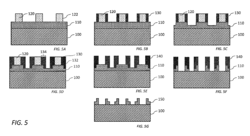
Swedish semiconductor startup’s APS™ patent portfolio continues to grow with new U.S. patent, marking the company’s 10th pending global patent.
Stockholm, Sweden – May 6th, 2025 – AlixLabs is excited to announce that the US Patent and Trademark Office has issued the notice of allowance for the company’s latest patent application, US20250087487A1, titled Formation of an array of nanostructures. This milestone marks the next step in AlixLabs’ commitment to advancing semiconductor manufacturing technologies.
Internally referred to as the “Tetris” patent, in honor of Alexey Pajitnov, the new patent integrates self-aligned double patterning (SADP) with atomic layer etching (ALE)-based pitch splitting (APS™) technology. This innovative approach, being industrialized by AlixLabs since its founding in 2019, combines elements of both classical and leading-edge techniques to deliver superior performance for semiconductor manufacturing.
The invention arose from AlixLabs’ efforts to develop a process for precise sidewall angle control in APS™, a key component in silicon-based processes. By leveraging plasma etch process selectivity and combining features from complex plasma processes, AlixLabs has pioneered a method that blends the traditional SADP process with the advanced APS technology.
This allows the company to utilize mature industrial technologies while benefiting from the advanced control and improved performance of cyclic processes and topographical selectivity. As a result, AlixLabs’ solution offers semiconductor manufacturers an enhanced ability to address the challenges of patterning at sub-5 nm nodes.
This breakthrough is significant for the integration of APS™ technology into existing semiconductor production workflows, preserving the use of existing Process Design Kits (PDKs) which are essential tools for chip designers. By doing so, it reduces the barrier for APS adoption in high-volume manufacturing (HVM), easing the transition to next-generation semiconductor technologies.
The patented innovation provides semiconductor manufacturers with greater flexibility, offering a new way to fine-tune the APS™ process to meet the needs to cut capital and operational expenditure (CapEx and OpEx) as well as emissions for customers at advanced technology nodes, while allowing for broader compatibility with different materials. This new method further strengthens AlixLabs’ core APS™ patent portfolio, positioning the company as a leading enabler of next-generation semiconductor manufacturing.
Moreover, this invention not only supports the development of leading-edge logic, memory, and photonics but also simplifies the semiconductor manufacturing process by reducing CapEx and OpEx for semiconductor fabs.
“We remain committed to advancing semiconductor manufacturing with innovations that significantly enhance the precision, flexibility, and efficiency of our technologies,” commented Dmitry Suyatin, co-founder and CTO of AlixLabs. “This patent represents a critical step forward in our mission to drive the next generation of semiconductor processes and further solidify our position as a leader in the field.”
April 10, 2025
AlixLabs to Demonstrate APS™ on 300-millimeter UMC wafers at the 2025 CMC Conference

Atomic Layer Etching Pitch Splitting (APS) proven on more industry-leading wafers, doubling fin density and proving flexibility without EUV.
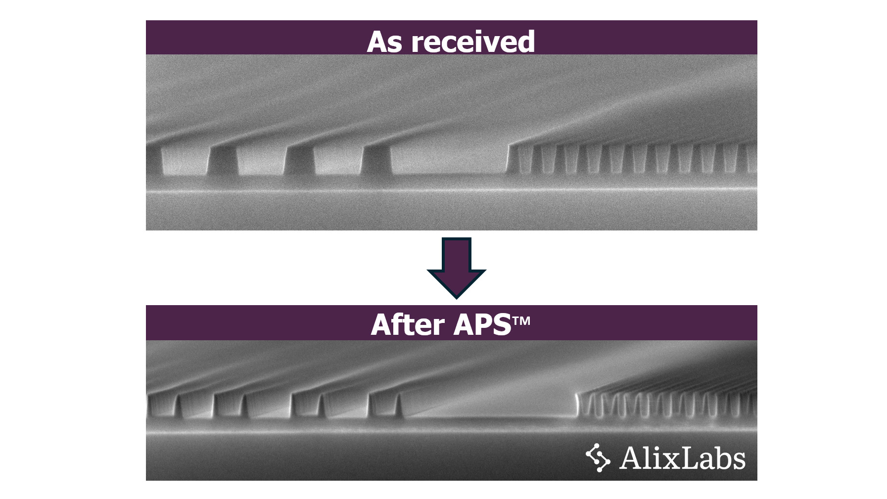
Austin, TX, USA/Stockholm, Sweden – April 10th, 2025 – AlixLabs AB, a Swedish semiconductor startup specializing in Atomic Layer Etching (ALE), today demonstrates the latest in its line of groundbreaking development in advanced chip fabrication unveiling additional research into its novel semiconductor manufacturing process known as APS™ (Atomic Layer Etching Pitch Splitting) capable of doubling fin density while introducing the unprecedented flexibility to vary pitch and critical dimensions within the same wafer area.
Proven on 300-millimeter wafers provided by United Microelectronics Corporation (UMC), the APS™ technology successfully halved pitch compared to current industry benchmarks. This significant advancement was achieved entirely without relying on expensive and energy-intensive Extreme Ultraviolet (EUV) lithography.
Instead, APS™ leverages advanced etching techniques that substantially enhance sustainability, drastically reducing energy consumption without compromising throughput. Previous demonstrations of the APS™ process, validated through Intel’s Test Vehicle Program[1], confirmed its potential by achieving metal pitches as small as 25 nanometers.
“Today we are sharing more proof that the APS™ process can be a game changer for leading foundries. Thanks to UMC, we have been able to verify our process on production wafers that are shipped in quantities measured in millions of wafers annually,” said Dr. Robin Athle, Principal Researcher at AlixLabs. “Our mission is to create equipment that allows companies that don’t have access to EUV tools to scale down their production to 5 nanometer and beyond. By eliminating the dependency on EUV lithography, we are offering the industry a path towards more sustainable and economically feasible high-density chip production.”
Detailed results from AlixLabs’ UMC wafer tests and further insights into APS™ technology will be presented at the 2025 CMC Conference, scheduled for April 10th in Austin, Texas. Dr. Athle’s presentation “Atomic Layer Etching Pitch Splitting (APS™): a New Alternative to Multi Patterning” will be held at 4:00 PM at the Bergstrom Ballroom in Hilton Austin Airport Hotel.
[1] https://www.alixlabs.com/2025/02/07/alixlabs-to-showcase-latest-aps-findings-at-spie-advanced-lithography-patterning/
February 7, 2025
AlixLabs to Showcase Latest APS™ Findings at SPIE Advanced Lithography + Patterning
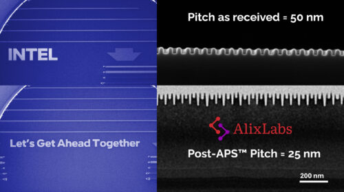
Swedish semiconductor startup to demonstrate 3-nanometer class FinFET structures made with APS™ on Intel Silicon at trade show.
Stockholm, Sweden – February 7th, 2025 – AlixLabs AB, a Swedish semiconductor startup specializing in Atomic Layer Etching (ALE), announces that it has used its APS™ (ALE Pitch Splitting) technology to etch structures corresponding to commercial 3-nanometer semiconductor processes on test silicon provided by Intel. The results will be shared in full by CTO and co-founder Dmitry Suyatin at the SPIE Advanced Lithography + Patterning trade show in San Jose, California, 23–27 February.
“We are excited to demonstrate how APS™ can help the industry lessen its reliance on multi-patterning solutions in Silicon Valley, while lowering costs and environmental impact. Our tech has been able to produce sub-10-nanometer class features on silicon, and with the help of Intel’s Test Vehicle Program we have proven that sub-5-nanometer class features are possible on mass-production silicon by just etching,” says Dmitry Suyatin, CTO and co-founder of AlixLabs.
AlixLabs APS™ achieved a 25 nm full metal pitch, comparable to 3-nanometer class technology from the leading foundries, on the Intel Low Global Warming Potential Etch Test Vehicle. This is a major milestone on the company’s road to commercialization, with further news to follow later in 2025.
“APS™ proves that there’s no need for complex multi-patterning like SADP and SAQP to produce 5 nanometer chips and beyond. It extends the potential of immersion lithography for use with critical mask layers for even 3-nanometer processes,” says Jonas Sundqvist, CEO and co-founder of AlixLabs. “These results were produced with our alpha tool, with a beta tool to follow later in 2025. We wish to thank Intel for providing leading-edge grade test silicon for this demonstration.”
For more information on the latest APS™ developments at SPIE Advanced Lithography + Patterning, make sure to attend Dmitry Suyatin’s presentation on February 27th, at 9:00–9:20 AM (PST).
February 4, 2025
AlixLabs Announces Research Collaboration with Linköping University

Swedish semiconductor startup and leading Swedish university to explore joint research in gallium nitride (GaN) and indium nitride (InN).
Stockholm, Sweden – February 4th, 2024 – AlixLabs AB, a Swedish semiconductor startup specializing in Atomic Layer Etching (ALE), announces that it has entered a research collaboration with Linköping University. The company and the university will join forces in furthering Swedish research into gallium nitride (GaN) and indium nitride (InN) deposition and etch, strengthening not only their own respective expertise in RF and power electronics but also aligning with the Swedish semiconductor sector.
“Our goal is to widen our research portfolio beyond deposition to etching, which is AlixLabs’ specialty,” says Henrik Pedersen, professor in inorganic chemistry at Linköping University. “During our initial research phase, we found that we have the same plasma etch equipment in our university labs as AlixLabs has at its home base in Lund, meaning we can run research in parallel. We look forward to exchanging information and know-how, especially in an all-Swedish collaboration.”
The resulting research will help strengthen AlixLabs’ offering within RF and power semiconductors, a field the EU has labeled as critical for its climate goals. It is a participant in the GaN-centered, Infineon-led, All2GaN project which underpins the union’s ambitions to achieve climate neutrality by the year 2050.
“We are excited about partnering up with the team at Linköping University and Professor Pedersen, a renowned researcher in the atomic layer deposition (ALD) and semiconductor chemistry space. Our goal is to find ways to qualify our processes for use in materials beyond silicon and we found significant synergies between our labs with regards to GaN and InN,” says Jonas Sundqvist, CEO and co-founder of AlixLabs.
Beyond leading-edge semiconductors, for which AlixLabs’ flagship APS™ process caters, the power electronics market is expected to grow significantly until the end of the decade, with Yolé Developpement forecasting an annual growth of revenue from power GaN devices of over 40 percent through 2029.
“Our etching processes have found a lot of interest among clients in the power electronics field. Ideally, our processes will have something to offer all players, no matter which semiconductor material they wish to process,” concludes Sundqvist.
December 11, 2024
AlixLabs at SEMICON Japan 2024

SEMICON Japan starts today, and AlixLabs is of course in the midst of the action. You will find our team in the EU Pavillion, booth 7201, where our COO and R&D Manager Amin Karimi and our business developers Rob Cadman and Masanori Sakuuchi.
Be sure to stop by for the latest info on APS™ and to hear the progress on our 300-millimeter equipment for the process. The show runs through Friday, December 13th.
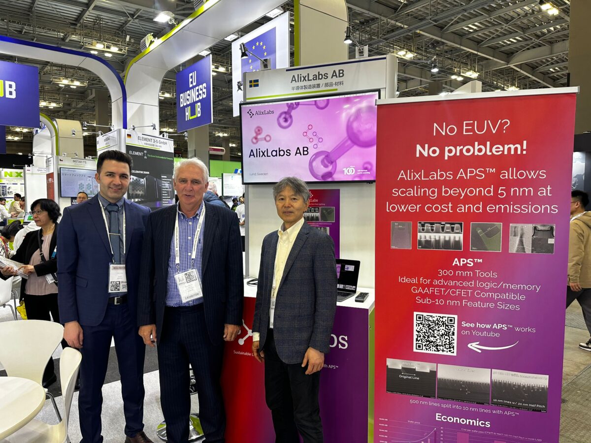
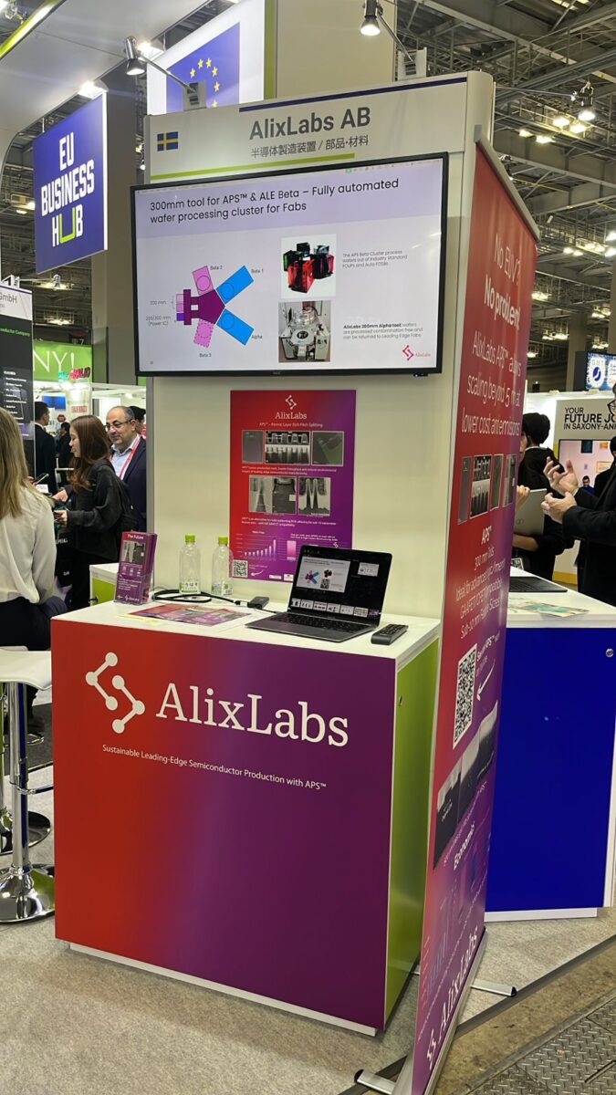

For more info on AlixLabs at Semicon Japan 2024, see our announcement.