


August 28, 2026
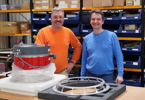
AlixLabs Sax Forma Beta Chamber Enters Final Assembly at VDL Projects
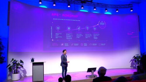
Lund, Sweden – August 28, 2026 – AlixLabs AB, a semiconductor equipment company specializing in advanced etch and patterning technologies, today announced that the assembly of its first Sax Forma Beta tool for Atomic Pitch Splitting, APS™, has commenced at VDL Projects, The Netherlands.
This milestone keeps AlixLabs on track to install the Sax Forma Beta tool in its own cleanroom by the end of 2026, enabling beta testing of APS™ for customers and partners.
The second Beta tool will enter the assembly phase as well before the end of this year. These developments are part of AlixLabs’ continued transition from technology validation toward deeper customer engagement, process integration, and industrial equipment deployment. Following the launch of Sax Forma, AlixLabs’ first commercially available APS™ System, the Sax Forma Beta tools represent the next step in preparing APS™ for evaluation in mass production environments.
“Starting the assembly of the Sax Forma Beta tool is an important commercial milestone for AlixLabs,” said Jonas Sundqvist, CEO at AlixLabs. “It means we are moving from demonstrating the core APS capability toward beta testing with customers where we can return contamination free wafers to the customer pilot lines and actual fabs. This is critical for process integration, showcasing manufacturing value, and the role APS can play in reducing patterning complexity and cutting cost for advanced semiconductor manufacturing.”
APS™ is designed as a complementary patterning system inserted downstream of established lithography-based process flows, including DUV, EUV, and nanoimprint lithography (NIL). By enabling controlled pitch splitting after the initial pattern has been defined, APS™ can increase pattern density without subsequent passes of lithography.
The Sax Forma Beta tools are being industrialized together with industry heavyweight VDL Projects, AlixLabs’ partner for system integration and high-tech equipment manufacturing. VDL Projects is supporting the transition of APS™ from advanced R&D and process validation into industrial equipment, drawing on its experience in design, engineering, realization, and scale-up of first-of-a-kind systems.
“Completing the design and engineering of the first-of-a-kind APS™ equipment on schedule has been a tremendous challenge,” said Sorin Stan, Senior Director for Emerging Technologies at VDL Projects. “We did not experience a single week of delay, which preserved the overall planning for the realization phase. The manufacturing and procurement of parts, the assembly currently underway, and the testing before shipment have been planned with half-day accuracy. This showcases our extensive experience in enabling ambitious, accelerated growth of both small and large companies at times when novel equipment is paramount to their success.”
Once installed in AlixLabs’ cleanroom, the Sax Forma Beta tools will support automated production-like APS™ demonstrations for customer evaluation, integration work, and validation on industry-relevant silicon design for logic and memory products at the advanced technology nodes. The beta testing will help semiconductor manufacturers assess how APS™ can be integrated into existing manufacturing flows while preserving fab infrastructure and reducing patterning complexity.
The Sax Forma Beta tools also support AlixLabs’ longer-term equipment roadmap, with additional deliveries scheduled for customers in 2027. The Beta tools also form an important step toward the company’s planned final high-volume manufacturing (HVM) Gamma platform targeted for 2028.
With the Sax Forma Beta tools now in full assembly, AlixLabs continues to advance APS™ toward commercial adoption as a semiconductor equipment platform for the Ångström era.
About AlixLabs
Established in 2019 in Lund, Sweden, AlixLabs emerged as a spin-off from Lund University with a mission to enable the cost-effective and energy-conscious fabrication of semiconductors, particularly logic and memory components. AlixLabs boasts patented recognition for its groundbreaking APS™ technique, a process that achieves nanostructure division through etching. This method holds approved patents across the USA, Taiwan, and Europe. The APS™ acronym signifies Atomic Pitch Splitting, leveraging ALE (Atomic Layer Etching), a plasma-based dry etching cyclic methodology. For more details, please visit www.alixlabs.com.
About VDL Projects
As part of VDL Groep of The Netherlands, VDL Projects has a proven track record in supporting innovative companies in the transition from the feasibility to the design, engineering, and realization of their equipment. With all needed expertise under one roof, VDL Projects scales up the equipment manufacturing from first-of-a-kind units to batch manufacturing, and further to turnkey realization of complex production lines. VDL Groep is an industrial conglomerate headquartered in Eindhoven, The Netherlands. It was founded in 1953 and consists currently of more than 100 specialized companies employing together more than 14,000 employees in 20 countries and operating in several industrial sectors. For more details, please visit https://www.vdlgroep.com/en.
August 6, 2026
AlixLabs Expands Footprint at RISE ProNano in Lund by 400 Square Meters

New capacity supports continued commercialization of APS™ technology and expanded beta testing for semiconductor customers.
LUND, Sweden — August 6, 2026 — AlixLabs AB, a Swedish semiconductor technology company pioneering Atomic Pitch Splitting, APS™, today announced that it is expanding its cleanroom space at the Lund-based RISE ProNano lab by 400 square meters.
The expansion is part of AlixLabs’ continuous growth plan as the company advances from technology development toward commercialization. The additional cleanroom capacity will provide AlixLabs with more space to install, qualify and operate equipment for customer-facing beta activities, including semiconductor wafer processing and process validation for leading semiconductor clients.
A central part of the expansion is preparation for the company’s APS Beta platform, which is expected to become operational in the second half of 2026. The platform will allow AlixLabs to run more extensive beta tests with semiconductor customers and support the transition of APS™ from pilot-scale development toward commercial manufacturing use cases.
“Expanding our cleanroom footprint at RISE ProNano is a significant step in our commercialization roadmap,” said Jonas Sundqvist, CEO of AlixLabs “The additional 400 square meters give us the infrastructure needed to scale our beta activities, support customer evaluations and demonstrate the value of APS™ in a production-relevant environment.”
AlixLabs’ APS™ technology is designed to enable advanced semiconductor patterning through a fast atomic layer etching (ALE) process, creating extremely small and precise structures while reducing process complexity. By expanding its cleanroom capacity, the company is strengthening its ability to support semiconductor customers as they evaluate new approaches to future chip manufacturing.
The expansion also reinforces AlixLabs’ long-term presence in Lund’s semiconductor ecosystem. Based at RISE ProNano, AlixLabs benefits from access to advanced infrastructure, process expertise and a collaborative environment designed to support the scaling of next-generation semiconductor technologies.
“This expansion is not only about more space,” added Sundqvist. “It is about building the operational foundation required for commercialization. With the APS™ Beta platform coming online later this year, we are creating the capacity needed to work more closely with customers and accelerate the path toward industrial adoption.”
About AlixLabs
Established in 2019 in Lund, Sweden, AlixLabs emerged as a spin-off from Lund University with a mission to enable the cost-effective and energy-conscious fabrication of semiconductors, particularly logic and memory components. AlixLabs boasts patented recognition for its groundbreaking APS™ technique, a process that achieves nanostructure division through etching. This method holds approved patents across the USA, Taiwan, and Europe. The APS™ acronym signifies Atomic Pitch Splitting, leveraging ALE (Atomic Layer Etching), a plasma-based dry etching cyclic methodology. For more details, please visit www.alixlabs.com.
June 23, 2026
AlixLabs launches Sax Forma for the Ångström era
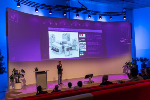
Lund, Sweden – June 23, 2026 – AlixLabs AB, a semiconductor equipment company specializing in advanced etch and patterning technologies, launched Sax Forma, an APS™ System, the company’s first commercially available equipment platform for Atomic Pitch Splitting (APS).
The launch marks AlixLabs’ transition from technology validation toward customer engagement, process integration, and industrial equipment deployment. Sax Forma is designed to bring APS™ into advanced semiconductor manufacturing flows, where continued scaling increasingly depends on reducing patterning complexity.
“With Sax Forma, we are taking APS from validated technology to a commercially available equipment platform,” said Jonas Sundqvist, CEO at AlixLabs. “This is an important step for AlixLabs as we begin deeper customer engagement around how APS can be integrated into existing manufacturing flows and support the industry’s continued scaling roadmap.”
Patterning has become one of the most cost-sensitive and technically demanding areas of advanced chip production, as scaling increasingly requires multi-patterning, additional process loops, and tighter control of critical dimensions, overlay, film thickness, and profile. APS addresses this challenge as a complementary patterning system inserted downstream of established lithography-based process flows, including DUV, EUV, and nanoimprint lithography.
By increasing pattern density without requiring a new lithography platform, APS enables fabs to reduce patterning complexity while preserving existing fab infrastructure and manufacturing investments.
Sax Forma builds on APS demonstrations using industry-relevant silicon, including 300 mm silicon wafers from UMC and Intel FinFET test silicon. On the Intel test silicon, APS reduced the half-pitch from 25 nanometers to 12.5 nanometers, demonstrating performance relevant to geometries associated with the 3-nanometer class. In laboratory settings, AlixLabs has also shown that sequential APS processing can enable further half-pitch reduction, pointing toward future scaling as the industry moves toward 2-nanometer, Ångström-class nodes, and beyond.
Together, these demonstrations support AlixLabs’ core claim: that APS can enable controlled half-pitch refinement in dense, line-based patterning layers without relying on repeated spacer-based process loops.
“APS is designed to complement lithography by adding a controlled pitch-splitting step after the initial pattern has been defined,” said Amin Karimi, CTO at AlixLabs. “The objective is to reduce patterning complexity while preserving compatibility with established process flows. That integration model is central to how we see APS being adopted by semiconductor manufacturers.”
Sax Forma is being industrialized together with VDL ETG Projects, AlixLabs’ partner for system integration and high-tech equipment manufacturing. Building on the collaboration announced earlier this year, VDL ETG Projects is supporting the transition of APS from advanced R&D and process validation into industrial equipment, drawing on its experience in design, engineering, realization, and scale-up from first-of-a-kind systems toward batch manufacturing.
AlixLabs has also built a strong and growing patent portfolio around APS and its equipment platform. The core APS principle is patent protected in key semiconductor markets including the EU, the United States, and Taiwan, while the company expects its process optimization work and hardware innovations to be covered by nine and eleven patent families, respectively, by the end of the year.
Sax Forma enters the market as AlixLabs’ Beta system, intended for customer evaluation, integration work, and validation in production-like environments. As the first commercially available APS equipment platform, it forms the basis for the company’s planned Gamma platform, targeted for 2028.
With Sax Forma, AlixLabs is bringing APS to market as a semiconductor equipment platform that offers a solution to one of the industry’s central scaling challenges: reducing patterning complexity on the path toward the Ångström era.
About AlixLabs
Established in 2019 in Lund, Sweden, AlixLabs emerged as a spin-off from Lund University with a mission to enable the cost-effective and energy-conscious fabrication of semiconductors, particularly logic and memory components. AlixLabs boasts patented recognition for its groundbreaking APS™ technique, a process that achieves nanostructure division through etching. This method holds approved patents across the USA, Taiwan, and Europe. The APS™ acronym signifies ALE Pitch Splitting, leveraging ALE (Atomic Layer Etching), a plasma-based dry etching cyclic methodology.
May 7, 2026
AlixLabs to host APS™ System Launch Event in Eindhoven on June 4
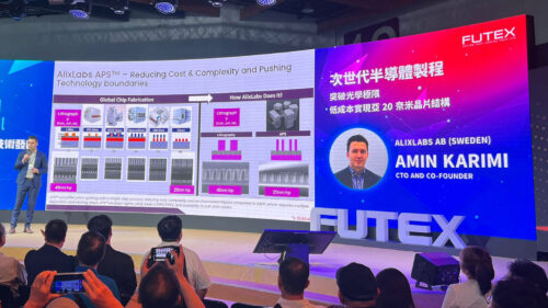
Lund, Sweden – May 7th, 2026 – AlixLabs will host the official launch event for its APS™ (Atomic Pitch Splitting) System, gathering guests from across the semiconductor ecosystem at High Tech Campus Eindhoven in the Netherlands.
The event marks an important milestone in AlixLabs’ transition from technology validation toward industrial deployment, as the company moves to introduce APS™ as a new patterning approach for advanced semiconductor manufacturing.
As advanced semiconductor manufacturing faces increasing challenges related to patterning complexity, process cost and manufacturability, APS™ has been developed to enable advanced pitch division through Atomic Layer Etching-based integration schemes aimed at simplifying multi-patterning flows and reducing process complexity in advanced semiconductor manufacturing.
During the event, AlixLabs will present the APS™ system architecture, recent development progress and the broader industrial implications of the technology, including process integration, manufacturability and future scaling opportunities.
“APS™ has been developed with manufacturability and industrial scalability in mind from the beginning,” said Jonas Sundqvist, CEO and Founder of AlixLabs. “This event represents an important step as we continue expanding our ecosystem engagement and move toward future industrial implementation.”
The APS™ System Launch Event will take place on June 4, 2026 at High Tech Campus Eindhoven in the Netherlands, with registration opening at 15:00 CEST and the main program running from 16:00 to 18:00, followed by networking.
Event details:
Date: June 4, 2026
- Location: High Tech Campus Eindhoven, The Netherlands
- Registration opens: 15:00 CEST
- Main program: 16:00–18:00 CEST
- Networking session: 18:00 onwards
Due to limited venue capacity, registration is required. Additional information and registration details are available here:
About AlixLabs
Established in 2019 in Lund, Sweden, AlixLabs emerged as a spin-off from Lund University with a mission to enable the cost-effective and energy-conscious fabrication of semiconductors, particularly logic and memory components. AlixLabs boasts patented recognition for its groundbreaking APS™ technique, a process that achieves nanostructure division through etching. This method holds approved patents across the USA, Taiwan, and Europe. The APS™ acronym signifies ALE Pitch Splitting, leveraging ALE (Atomic Layer Etching), a plasma-based dry etching cyclic methodology.
April 14, 2026
AlixLabs Closes 15 M EUR Series A with Strategic Investment from Stephen Industries

Lund, Sweden – April 14th, 2026 – AlixLabs, a pioneer in Atomic Layer Etching (ALE) technology for next-generation semiconductor manufacturing, today announced that it closed its 15 million euro Series A in the first quarter of 2026 following a strategic investment from Stephen Industries, a Finnish investment company with a strong track record in scaling advanced technology ventures.
In November 2025, AlixLabs announced that Global Brain and key institutional investors had subscribed to its Series A to the tune of 14,1 million euro, with the difference to the 15 million total remaining open until the first quarter of 2026.
The investment marks a strategic milestone for AlixLabs as it continues to develop its proprietary ALE solutions with especially its flagship APS™ (Atomic Pitch Splitting) technology aimed at enabling more precise, efficient, and cost-effective semiconductor fabrication.
A key dimension of the partnership is the involvement of Kustaa Poutiainen of Stephen Industries, whose experience in building and scaling deep-tech companies brings significant strategic value. Poutiainen previously played a central role in the growth of Picosun, a Nordic Atomic Layer Deposition (ALD) company that became a global leader in its field. Given the close technological relationship between ALD and ALE, this track record is particularly relevant to AlixLabs’ mission.
“Stephen Industries brings deep industrial expertise and a proven ability to scale companies in adjacent technology domains,” said Jonas Sundqvist, CEO of AlixLabs. “Kustaa’s experience with Picosun is especially valuable as we move from development toward broader commercialization of our APS™ platform.”
Atomic Layer Etching is widely seen as a critical enabler for future semiconductor nodes, complementing ALD processes by allowing atomic-scale precision in material removal. As device architectures become increasingly complex, ALE is expected to play a central role in manufacturing.
“AlixLabs operates in a highly promising space within semiconductor process technology,” said Kustaa Poutiainen, Chairman and President of Stephen Industries. “Having seen firsthand how ALD evolved from a niche innovation to a critical industry standard, I see strong parallels with ALE. AlixLabs has the potential to follow a similar trajectory.”
The new funding will be used to accelerate product development, expand technical capabilities, and strengthen partnerships with semiconductor manufacturers.
This investment reinforces AlixLabs’ position as a key innovator in the European semiconductor ecosystem and supports its ambition to become a global leader in Atomic Layer Etching.
Older articles
November 27, 2024
AlixLabs to Debut 300-millimeter Equipment at SEMICON Japan
Swedish semiconductor startup premieres 300-millimeter APS™ for advanced logic and memory, steps up business development efforts in Japan.
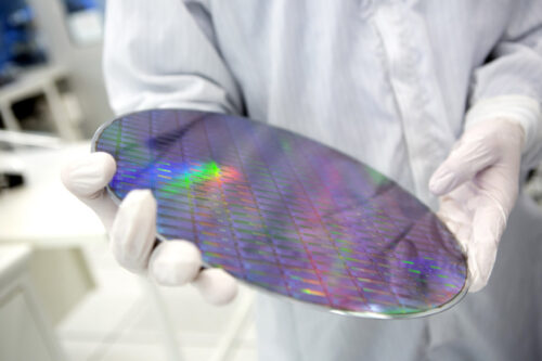
Stockholm, Sweden – November 27th, 2024 – AlixLabs AB, a Swedish semiconductor startup specializing in Atomic Layer Etching (ALE), announces its participation at SEMICON Japan 2024, marking the public debut for the company’s 300-millimeter wafer process chamber. Its Made in Sweden APS™ (ALE Pitch Splitting) tools are aimed at allowing the semiconductor industry to scale down to sub-7-nanometer manufacturing processes in a more sustainable way, and is positioned as an alternative to costly double patterning or EUV (extreme ultraviolet) solutions.
AlixLabs APS™ is designed to reduce the cost of leading-edge manufacturing, sub-7-nanometer, where feature sizes of less than 20 nanometers are required. An estimated cost saving of up to 40 percent per mask layer can be achieved with APS™ rather than relying on EUV lithography, and complex self-aligned multi patterning schemes.
“As our 300-millimeter tool is being put through its paces in our lab, we look forward to demonstrating it for Japanese clients. Japan is investing heavily in revitalizing its semiconductor industry and once again becoming a leading-edge player in the business. With APS™ we can help make this happen at lower costs up front as well as during mass production, while we lower the carbon footprint of the production,” says Amin Karimi, COO and R&D Manager at AlixLabs. “At the show, I’m personally looking forward to meeting existing and prospective clients and being part of the Japanese semiconductor buzz. We have a lot of interest from Japanese clients, and it’s the place to be for us.”
APS™ and the Made in Sweden tools associated with it can already create 20-nanometer half-pitch lines and critical dimensions below 15 nanometers on silicon and 3 nanometers on gallium phosphide. It also has numerous applications for power electronics, including precision etching and surface cleaning, each allowing for improved electrical performance than conventional methods in use today.
AlixLabs’ goal is to supply leading semiconductor manufacturers, in both logic and memory segments. At SEMICON Japan, it will be represented by COO and R&D Manager Amin Karimi in the EU Pavilion.
November 18, 2024
AlixLabs Awarded 345,000€ Swedish Innovation Agency Grant
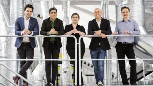
Funds awarded from Swedish innovation agency’s “Acceleration of deep tech companies 2024” call
Stockholm, Sweden – November 18th, 2024 – AlixLabs AB, a Swedish startup pioneering advanced semiconductor solutions, has been granted 4 MSEK in funding from Swedish innovation agency Vinnova, equivalent to approximately 345,000 EUR. The funding is spread out over three years with 658,000 SEK (~56,000 EUR) credited immediately, with the remainder to follow over the coming three years. The funds will help AlixLabs’ further its APS™ technology to a higher Technology Readiness Level (TRL) and strengthen customer engagement efforts.
The funding is part of Vinnova’s initiative to accelerate deep tech companies, recognizing the potential of AlixLabs’ APS™ technology to enable cost-efficient Ångström-level scaling for the semiconductor industry.
“We are always pleased to receive recognition and state support for our efforts to scale up our business and commercialize our technology,” said Amin Karimi, COO and R&D Manager at AlixLabs. “The support comes at a crucial stage as we are installing our first 300-millimeter tool in our clean room and are increasingly engaging with potential clients around the semiconductor industry. At the core of our efforts is our APS™ technology which we are convinced is the most sustainable and affordable way forward for semiconductor manufacturing at 3 and 2 nanometers and beyond.”
AlixLabs’ offering includes its APS™ technology (Atomic Layer Etch Pitch Splitting) that already allows for etching of feature sizes comparable to those of today’s 3-nanometer class chips with the company’s own equipment. With other proprietary ALE (Atomic Layer Etching) processes, AlixLabs can also contribute to RF and Power IC Gallium Nitride (GaN) and Silicon Carbide (SiC) workflows, with pattern transfer, precision etching and surface roughness reduction for wafers.
“The semiconductor industry is facing a big challenge with regards to sustainability and rising costs to manufacture leading-edge semiconductors. We propose etching instead of costly EUV lithography, and our demonstrations show that we can help produce sub-3-nanometer chips at 35–50 percent lower costs per wafer pass than by using EUV,” said Jonas Sundqvist, CEO at AlixLabs. “While we target the leading-edge logic and memory producers with APS™, our technology also makes it possible for foundries who have given up pursuing sub-20-nanometer production to scale down in a cost-effective way.”
The Vinnova grant will be used by AlixLabs to accelerate the commercialization of its APS™ technology by deepening customer engagement and conducting demonstration projects. These demos will be carried out both at AlixLabs’ facilities and on customer platforms, showcasing the practical advantages of APS™. This approach is expected to advance the Technology Readiness Level (TRL) of our solutions, paving the way for broader industry adoption and reinforcing AlixLabs’ commitment to delivering innovative, cost-effective scaling solutions for semiconductor manufacturing.
October 23, 2024
AlixLabs’ APS™ Delivers 10 nm Precision & Cost Savings
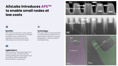
Please amaze yourself by our Disruptive APS(TM) Technology. Here we show critical dimensions (CDs) of 10 nm in an amorphous silicon mask at a 20 nm Half Pitch – that´s like butter on the bread in semiconductor manufacturing used multiple times in the manufacturing of several chips in your phone.
One of the reasons why your phone is so expensive is that those chips are made with several masks using Extreme Ultra Violet Lithography (EUV) and other masks using extremely complicated Self-Aligned Quadruple Patterning (SAQP) – AlixLabs APS(TM) aims to change that!
September 30, 2024
AlixLabs 2024 World Tour

AlixLabs is happy to announce that our 300 mm APS™ Alpha Tool is now in its final testing phase. For those interested in investing in our Series A 300 mm Beta Cluster Tool Phase or partnering with us in our innovative APS™ technology, we invite you to schedule a one-on-one web update through (Contact – AlixLabs).
Alternatively you can meet us face-to-face during our AlixLabs World Tour 2024, which includes stops across Asia (Japan, Korea, Taiwan) in early October, the East Coast USA in early October and Florida for AVS70 from November 3-8. Later in October and into December we will be visiting Taiwan, Korea and Japan again, including SEMICON Japan. You can also meet us in the Netherlands on October 21-22 or at SEMICON Europa in Germany this November.
We would also love to welcome you for a Swedish fika in Lund—let’s connect!
September 12, 2024
AlixLabs Qualifies APS™ for Use In 300-millimeter Silicon Wafer Designs and the Ångström (Å) era
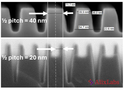
Swedish semiconductor startup clears technical hurdle for leading-edge process use on 300 mm wafer design.
Stockholm, Sweden – September 12th, 2024 – AlixLabs AB, a Swedish semiconductor startup specializing in Atomic Layer Etching (ALE), announces that it has qualified its APS™ (ALE Pitch Splitting) process on a 300-millimeter silicon wafer design, marking one of its final steps towards commercial adoption. APS™ provides atomic-scale precision and pattern fidelity with critical dimensions below 15 nanometers for both single crystalline and amorphous silicon.
AlixLabs APS™ is designed to reduce the cost of leading-edge manufacturing, sub-7-nanometer, where feature sizes of less than 20 nanometers are required. An estimated cost saving of up to 40 percent per mask layer can be achieved with APS™ rather than relying on EUV lithography, and complex self-aligned multi patterning schemes.
“Proving that APS™ works on lithography designs on 300-millimeter wafers, is what we’ve all worked on since we founded AlixLabs in 2019,” says CEO and co-founder Dr. Jonas Sundqvist. “Not only do we aim to provide chip manufacturers wafer processing equipment that can create 20-nanometer half-pitch lines and critical dimension below 15 nanometers on silicon, we aim to do that at a lower cost and a more sustainable way than other technologies”
“We are also able to provide record breaking 3-nanometer critical dimension features on gallium phosphide (GaP) wafers today showing that APS™ can scale far into the future beyond what is needed today,” adds CTO and co-founder Dmitry Suyatin.
APS™ is positioned as an alternative to self-aligned double and quadruple patterning (SADP and SAQP). It allows for splitting dense line structures that can act as a foundation for transfer-etch into various materials such as dielectrics, metals, metal nitrides, and high-k dielectrics. The structures created with APS™ can also be used as-is for critical device features such as the fins in FinFET-type transistors due to extremely low surface damage.
AlixLabs’ goal is to supply leading semiconductor manufacturers, in both logic and memory segments. By enabling them to simplify and speed up their chip production at least fourfold for each critical mask layer by replacing four plasma wafer processing chambers in the SADP process flow with one APS™ chamber and eightfold correspondingly in SAQP. Finally, AlixLabs contributes overall to more sustainable semiconductor manufacturing.
July 3, 2024
AlixLabs awarded PhotonHub research grant
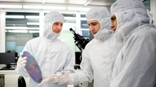
Swedish semiconductor startup now part of pan-European photonics innovation hub
Stockholm, Sweden – July 3rd, 2024, AlixLabs AB, a Swedish semiconductor startup specializing in Atomic Layer Etching (ALE), announces its expansion into the photonics field thanks to a new research grant from the imec-led and EU-supported PhotonHub Europe. The total value of the research project is approximately 197,000 euro, of which PhotonHub will provide 58,500 euro, with AlixLabs itself investing 129,000 euro.
The R&D project with PhotonHub Europe will allow for AlixLabs to work closely with the European Union’s most prolific semiconductor research hub imec, granting access to photonics equipment and technology not present at AlixLabs’ headquarters in Lund, Sweden. The project also enables AlixLabs to evaluate, prototype and benchmark its technology and processes in imec’s laboratories, qualifying them for worldwide industry use.
“Photonics is a hot topic in the future of semiconductor industry, and we are eager to explore application of our technology in this field,” said Reza Jafari Jam, Research Director at AlixLabs. “We’re thrilled about the opportunity to collaborate closely with imec and tap into the vibrant hub of European semiconductor research, enhancing our capabilities in developing high-performance photonic devices. Our passionate team is looking forward to pushing the technology’s boundaries with our innovative solutions and contribute to better communication, computing and medical technologies.”
The goal of the project is to significantly enhance the performance of photonic devices, particularly ring resonators. With AlixLabs’ ALE process, which allows for precise material manipulation at an atomic scale, the goal is to achieve defect and damage-free surfaces for photonics devices. As surface quality directly contributes to better photon extraction and transmission, ALE in photonics is expected to result in more reliable devices with higher signal quality and enhanced operational qualities.
PhotonHub Europe was announced in 2020 and is funded by the EU’s Horizon 2020 program. It has 54 partners and over 500 experts from 15 EU member states, all aiming to create and launch new products in industries as diverse as Health, Digital Infrastructure, Manufacturing, Safety, Security, Space & Defence, Agro-Food and Mobility & Energy.
April 5, 2024
AlixLabs announces EU-wide APS Trademark
The European Intellectual Property Office grants Swedish semiconductor startup registration of the phrase APS (ALE Pitch Splitting).
Stockholm, Sweden – April 5th, 2024, AlixLabs AB, a Swedish semiconductor startup specializing in Atomic Layer Etching, announces that it has been granted a certification of registration for its trademark APS by the European Union Intellectual Property Office. The acronym APS stands for Atomic Layer Etching (ALE) Pitch Splitting and describes the company’s revolutionary process that aims to enable the semiconductor industry produce chips of the future at Ångström scale (1Å = 0.1 nanometer) at lower cost and energy use.
“As we are nearing commercialization of our technology on 300-millimeter (12-inch) silicon wafers, it feels great to finally have a unique trademark to our unique semiconductor manufacturing process,” comments Jonas Sundqvist, CEO of AlixLabs. “We have been etching transistor fins since 2019, and within the upcoming quarters we will have fully validated the APS process on 300-millimeter wafers with new equipment developed by our fellow countrymen at Nanovac.”
Having previously demonstrated APS on bulk silicon, AlixLabs aims to install the new Nanovac-developed equipment in the summer of 2024. Once up and running, the goal is to finalize a commercial APS process that can be licensed to leading-edge semiconductor manufacturers to enable cheaper, more energy-efficient and sustainable production of advanced chips.
“This 300-millimeter wafer tool combines our deep industry knowledge with practical design innovations, aiming to offer improved precision and efficiency in semiconductor manufacturing,” says Thomas Engstedt, founder and CEO at Nanovac. “It’s a disruptive step forward for Atomic Layer Etching and APS processing, setting a solid foundation for future advancements by employing modular design concepts.” APS is the first trademark of AlixLabs, joining the company’s growing portfolio of patents related to the APS process that includes x European, x U.S. and x Taiwanese patents.
May 25, 2023
AlixLabs an ALL2GaN EU Project participant

AlixLabs is participating in the ALL2GaN EU project with your low-damage Atomic Layer Etch process technology. This collaboration with Infineon and other partners demonstrates a collective effort towards sustainable technology development and the use of innovative solutions like gallium nitride to enhance energy efficiency and reduce carbon emissions on a global scale.
The European Union’s Green Deal is a significant initiative aimed at achieving climate neutrality in Europe by 2050. This objective requires the development of smart, low-emission technologies and the promotion of a digitally advanced, competitive, and sustainable industry.
Research and innovation in power electronics, such as pacemaker technologies, are pivotal in driving the implementation of the Green Deal. These advancements enable energy-efficient and environmentally friendly solutions across various sectors, aligning with the goals of the EU’s sustainable agenda.
By investing in power electronics research and innovation, the EU can accelerate the adoption of sustainable technologies, contributing to a substantial reduction in carbon emissions and facilitating a greener and more sustainable future for the continent.
For more info, see the ALL2GaN website and Infineon’s press release.