April 7, 2026
AlixLabs and VDL ETG Projects Announce MoU for APS™ Patterning Technology Industrialization
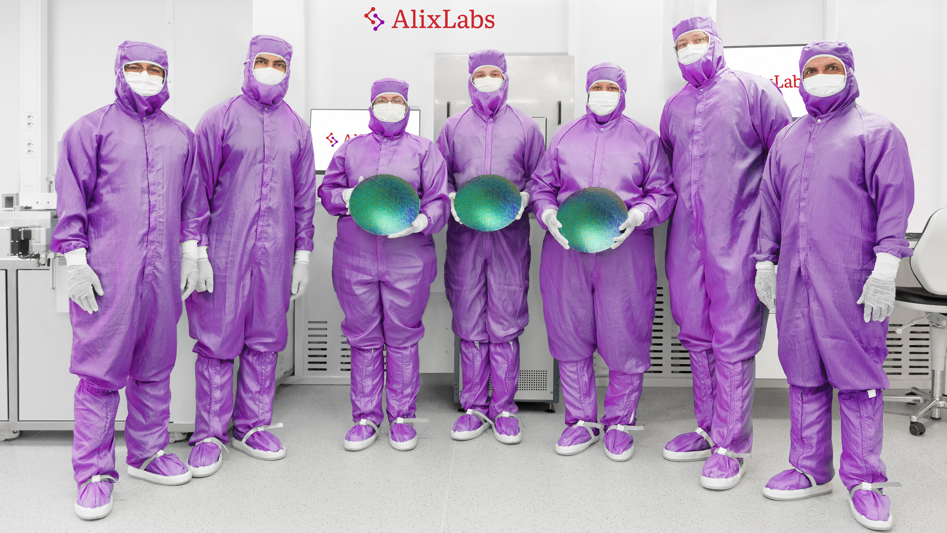
Lund, Sweden – April 7th, 2026 – AlixLabs AB, a semiconductor equipment company specializing in Atomic Layer Etching (ALE) innovations, today announced that the company has signed a Memorandum of Understanding (MoU) with VDL ETG Projects, part of VDL Groep, to advance the production of APS™ (Atomic Pitch Splitting) equipment.
The agreement marks a significant step toward industrializing AlixLabs’ APS™ technology, enabling scalable manufacturing solutions for advanced semiconductor patterning.
APS™ is designed to address critical challenges in next-generation semiconductor fabrication by enabling precise pitch splitting through atomic layer etching. This approach offers a cost-efficient and energy-conscious alternative to increasingly complex multi-patterning and EUV-based lithography.
Under the MoU, VDL ETG Projects will play a key role in developing and manufacturing the industrial APS™ tools, leveraging its expertise in system integration and high-tech equipment manufacturing. The collaboration aims to transition APS™ from advanced R&D into robust, production-ready systems for semiconductor fabs.
“This MoU represents an important milestone for AlixLabs as we move from technology validation toward industrial deployment,” said Jonas Sundqvist, CEO of AlixLabs. “Partnering with VDL ETG Projects strengthens our ability to scale APS™ and bring a new patterning paradigm to the semiconductor industry. Their industrialization capabilities are a strong complement to our process innovation.”
Sorin Stan, Senior Director for Emerging Technologies at VDL ETG Projects added:
“The implementation of AlixLabs’ research in the manufacturing processes for advanced semiconductor devices will contribute to overall cost reductions and increased production speeds. The industrialization of the first-of-a-kind APS™ equipment currently under development for AlixLabs will play an essential role in fulfilling the next-node strategies at many of their customers.”
The partnership reflects a shared ambition to accelerate the adoption of innovative patterning technologies and support the semiconductor industry’s need for sustainable scaling.
About AlixLabs
Established in 2019 in Lund, Sweden, AlixLabs emerged as a spin-off from Lund University with a mission to enable the cost-effective and energy-conscious fabrication of semiconductors, particularly logic and memory components. AlixLabs boasts patented recognition for its groundbreaking APS™ technique, a process that achieves nanostructure division through etching. This method holds approved patents across the USA, Taiwan, and Europe. The APS™ acronym signifies ALE Pitch Splitting, leveraging ALE (Atomic Layer Etching), a plasma-based dry etching cyclic methodology.
About VDL ETG Projects
As part of VDL Groep of The Netherlands, VDL ETG Projects has a proven track record in supporting innovative companies in the transition from the feasibility to the design, engineering, and realization of their equipment. With all needed expertise under one roof, VDL ETG Projects scales up the equipment manufacturing from first-of-a-kind units to batch manufacturing, and further to turnkey realization of complex production lines. VDL Groep is an industrial conglomerate headquartered in Eindhoven, The Netherlands. It was founded in 1953 and consists currently of more than 100 specialized companies employing together more than 14,000 employees in 20 countries and operating in several industrial sectors. For more details, please visit https://www.vdlgroep.com/en.