APS™: Atomic Pitch Splitting
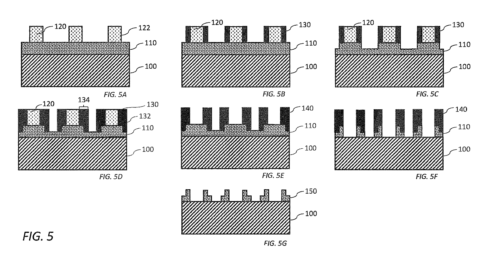
How It Works: AlixLabs’ Atomic Pitch Splitting (APS™) technology is a leading-edge process designed to enhance semiconductor manufacturing. The core of APS™ is the ability to split nanoscale features on semiconductor wafers into even smaller structures using an Extreme form of Atomic Layer Etching (ALE) in a simple, economical, and gentle way. This process leverages the unique properties of the sidewalls of nanoscale features, which act as a topographical mask during etching. By utilizing ALE, APS can accurately and efficiently create extremely fine features, with critical dimensions below 10 nm and a tight pitch, on silicon, dielectrics and other materials like gallium phosphide (GaP).
What It Is Good For: APS is highly beneficial in semiconductor fabrication, offering a method to continue scaling down chip components as per Moore’s Law while reducing costs and increasing the throughput. This process is particularly valuable because it allows manufacturers to achieve smaller, more densely packed components without the need for multiple complex lithography steps, which are both expensive and resource-intensive. The APS process thus reduces the capital investment, energy consumption, and the overall environmental impact of semiconductor production.
Applications: APS has broad applications in the semiconductor industry, particularly in the production of advanced logic and memory chips. It is complementary to existing lithography techniques, such as Deep Ultraviolet (DUV) and Extreme Ultraviolet (EUV) lithography and Self-Aligned Double and Quadruple Patterning (SADP and SAQP), but offers a simpler and more cost-effective alternative. This makes APS especially useful in the manufacturing of next-generation integrated circuits and memory devices, where precision at the nanoscale is critical. Furthermore, APS may play a significant role in sustainable semiconductor manufacturing, enabling high-performance chips while minimizing the environmental footprint.
This innovative process by AlixLabs is not only a breakthrough in semiconductor manufacturing but also a strategic step toward more sustainable and cost-effective production, making it a crucial tool for the future of electronics