Atomic Layer Etching (ALE) Pattern Shaping is a precision etching technique that selectively removes unwanted material from the surface of semiconductor structures.
Atomic Layer Etching (ALE) Surface Smoothening is an advanced etching technique developed by AlixLabs to enhance the surface quality of semiconductor materials, particularly GaN (Gallium Nitride) and SiC (Silicon Carbide).
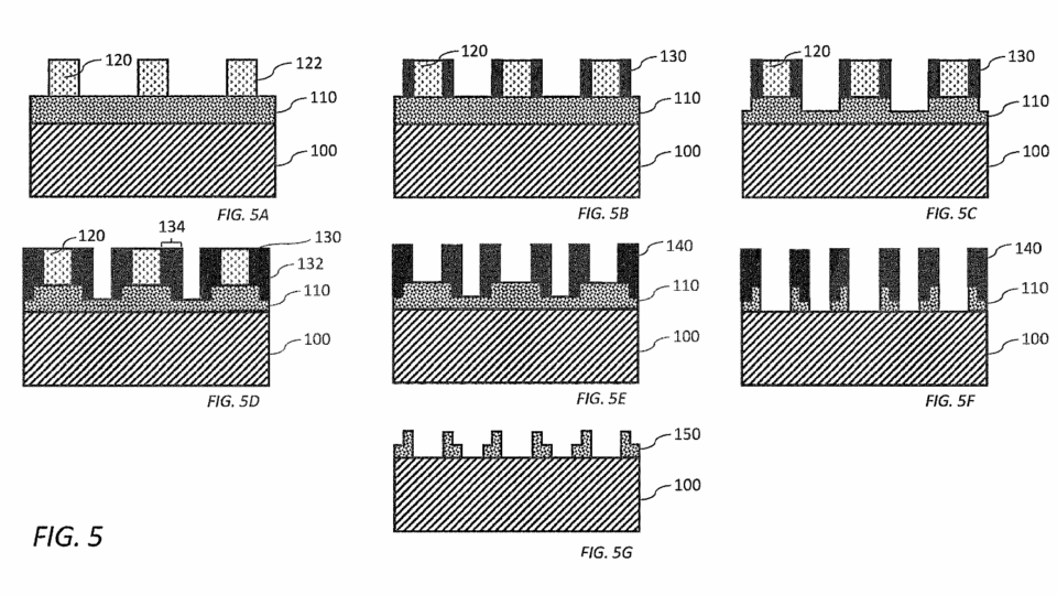
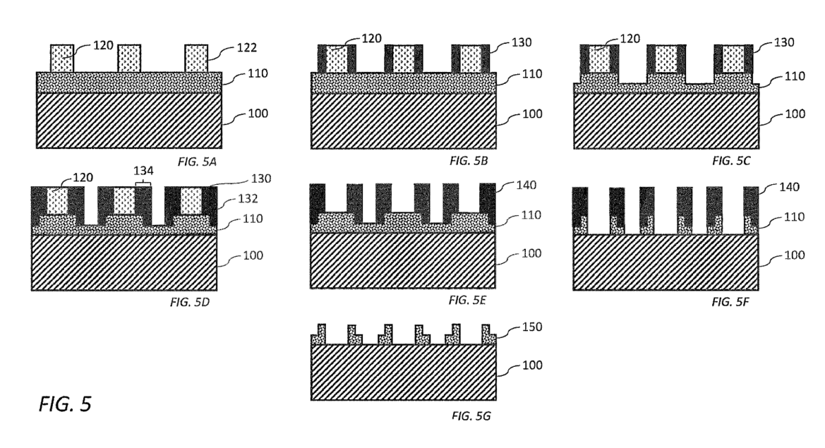
AlixLabs' Atomic Pitch Splitting (APS™) technology is a leading-edge process designed to enhance semiconductor manufacturing. The core of APS™ is the ability to split nanoscale features on semiconductor wafers into even smaller structures using an Extreme form of Atomic Layer Etching (ALE).